For contact info, please see the Sci.Electronics.Repair FAQ Email Links Page.
Copyright © 1994-2016
Reproduction of this document in whole or in part is permitted if both of the
following conditions are satisfied:
1. This notice is included in its entirety at the beginning.
This document provides detailed instructions for assembling the SG-µMD1
PCB Version 1.2.
A similar document is available for V1.0.
(There is no V1.1.) V1.0 and V1.2 are functionally equivalent for µMD1
in that they can be swapped in a system or substituted for the original
chipKit DP32 version without requiring
any hardware or software changes. Most of the differences
relate to the LED indicators, the majority of which are not
useful for µMD1 anyhow. :) But the correct assembly
procedure must be used because the layout has changed slightly,
along with some part numbers. Check the marking on the PCB to confirm
the version. All the kits should use the V1.2 PCB since I've already
populated all the V1.0 PCBs and there is only a single blank one remaining
for my reference. :)
The chipKit LEDs LED1-LED4 (on signals RB3-RB0) are still present
on SG-µMD1-V1.2 but their locations have changed as follows:
Of all the LEDs, only LD4 and LD0 are actually
needed. LD4 (LED1) flashes to indicate that the boot loader is
active. And LD0 (Power) is a key part of Smoke Test #1, below. ;-)
However, LD5 (LED3) may be used by the firmware as a heartbeat or for
status, so installing it is worthwhile. Beyond that, the other three
LEDs make the thing look like a Crhistmas tree. :) However, LD1-LD4
do monitor activity on REF, MEAS1, MEAS2, and MEAS3 so they could
conceivably have value when troubleshooting signal paths.
All components are through-hole and except as noted in the detailed
assembly procedure, should seat flush on the
PCB. They shouldn't be suspended in mid-air swinging in the breeze. :)
Most components are identified on the silk-screen and with only a few
exceptions, the label won't be obscured when the part is installed.
A low power soldering iron with narrow tip and thin (e.g., #22 AWG) rosin-core
solder will be required. DO NOT even think about attempting this without
suitable soldering equipment. It's well worth the investment. A Weller
soldering gun or propane torch will not work. :) Rosin core solder is also
essential. And while
I'm quite confident that you never make mistakes, a means of component removal
such as a de-soldering pump (e.g., SoldaPullt™) will be highly desirable.
Screwing up component removal can easily ruin the PCB and is not covered
under the unlimited limited warranty. :-)
Proper soldering technique will be such that the exposed solder on each
pad should be shiny with a concave profile. It should not be a blob and
just needs to fill the hole. Solder is not glue.
Some excess solder doesn't hurt anything
but looks unprofessional. A 10X magnifier may come in handy for
inspection. Residual rosin can be cleaned off with
isopropyl alcohol or an environmentally-friendly electronic solvent.
However, leaving the rosin alone is also acceptable (if ugly).
Total assembly time should be well under two hours for someone proficient
in fine soldering. Cutting component leads to 1/4 to 3/8 inch before
installation will simplify soldering as the long leads won't be poking
you in the face. :( :) Then trim flush after soldering.
It is recommended that the USB driver and µMD1 GUI be installed on
your PC or laptop prior to assembly so that it will be possible to perform
a "live" test as soon as the board is ready.
All Rights Reserved
2. There is no charge except to cover the costs of copying.
DISCLAIMER
µMD1 is intended for use in hobbyist, experimental, research, and other
applications where a bug in the hardware, firmware, or software, will not
have a significant impact on the future of the Universe or anything else.
While every effort has been made to avoid this possibility, µMD1 is an
on-going development effort. We will not be responsible for any consequences
of such bugs including but not limited to damage to the wafer FAB you
picked up on eBay for $1.98 + shipping, financial loss from the use of
37 spools of ABS due to the office 3-D printer running overnight and
fabricating a part 25.4x
too large in all dimensions, or bruising to your pet's ego from any number
of causes directly or indirectly related to µMD1. ;-)
Acknowledgment
Thanks to Jan Beck for selecting the chipKIT DP32 and writing and testing
initial versions of the firmware and GUI. And for getting me interested
in actually being involved in this project. If anyone had told me
six months ago that I'd be writing code in C, MIPS assembly language,
and Visual Basic - and enjoying it (sort of) - I would have suggested
they were certifiably nuts. ;-) Jan maintains the master GUI source code
as well as slightly different versions of the firmware and a
development blog on the overall project.
And a version of the firmware providing basic readout of displacement
on any Bluetooth wireless device with a terminal APP, or with a bit
more polished presentation (though not the complete GUI) on Android devices,
may be found on Jan's Web site. See that and more under "References".
Introduction
The SG-µMD1 kit of parts includes everything necessary for a 3 axis
µMD1 readout without sensors, as well as most other parts
needed to populate the PCB to be more or less equivalent to the chipKit DP32.
  chipKit LED  SG-uMD1-V1.2 LED  Signal  Location
 ---------------------------------------------------
   LED1 Boot      LD4 MEAS3       RB3    Near U2
     LED2         LD3 MEAS2       RB2    Near U2
     LED3         LD5  --         RB1    Near HDR2
     LED4         LD2 MEAS1       RB0    Near U1
      --          LD1 REF         RB5    Near U1
      --          LD0 Power       VIN    Near IC2
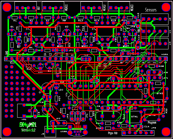
Schematic for the SG-µMD1 Version 1.2
The schematic for the SG-µMD1 Version 1.2 PCB may be found at
SG-µMD1 Version 1.2 Schematic.
This includes everything on the board. Minimally
Populated SG-µMD1 Version 1.2 Schematic includes only the
parts required for a system with up to three axes but no sensors. It
eliminates chipKIT DP32 features that are not needed for µMD1 and
is the version that will be of interest to most users. The other parts
can always be added at a later time if needed.
Printing out the schematic and having it available for reference while assembling the PCB may be helpful.
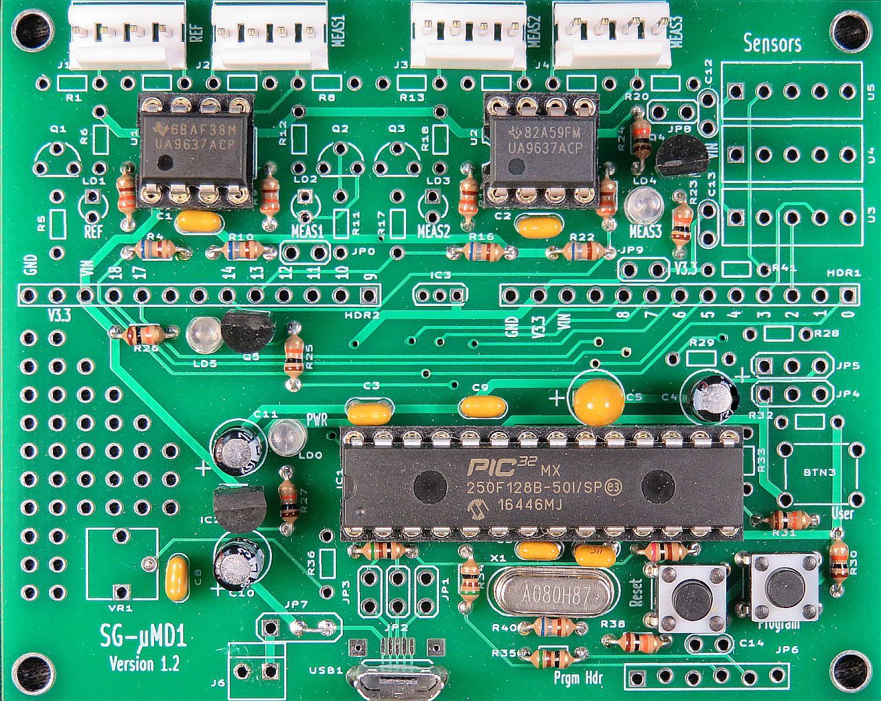
Click on the photo for a high resolution version which will open in a separate window for reference during assembly.
As can be seen by comparing this layout with that of the chipKIT board, most parts are in similar locations. The USB connector has moved to the bottom of the board along with its associated jumpers. The Arduino headers have moved slightly and there are now complete layout patterns for up to 3 measurement channels and locations for the environmental sensors.
For use with environmental sensors, additional components will be required that are not part of the standard SG-µMD1 kit.
The populated PCB shows all components required for a three axis system without sensors. The terminating resistors (R1,R2,R7,R8,R13,R14,R19,R20) have not been installed since their value may depend on the specific configuration. The hole spacing is such that a machine pin header strip with unused pins popped out can be installed so that resistors can be plugged into it.
IMPORTANT: All the resistors are labeled using the standard color coding as shown in the main µMD1 manual and below. Normal color vision is required to be able to identify these reliably. Even then, it is sometimes difficult to confirm the values that differ in one band or in poor lighting. And a magnifier may be required to read some markings on these and other components. If in doubt, have someone else assemble the kit or assist you.
For those not familiar with the common resistor color code (Black/0, Blown/1, Red/2, Orange/3, Yellow/4, Green/5, Blue/6, Violet/7, Gray/8, White/9), the resistors near the small IC in the upper left of the photo of the SG-µMD1 PCB shown above are 680 (blue-gray-brown or 68 with 1 zero) ohms and 330 (33 with 1 zero) ohms. The gold stripe indicates 5 percent tolerance on the value but for the use here, tolerance doesn't matter. (It's possible the resistors you use will have 4 stripes where 3 of them are the value and the 4th is the multiplier, along with one for tolerance. If in doubt confirm the value with a multimeter.) The chart below is from Digikey. (If the link decays, a Web search will readily find another one.)

The LEDs in the area for MEAS2 and MEAS3 are equivalent to the chipKit DP32 LED2 and LED1, respectively.
If only interested in running the PIC32 for other purposes, or for downloading the bootloader or other firmware using MPLAB, it's even simpler. Go to Assembly Instructions for the SG-µMD1 for MPLAB Version 1.2 PCB.
OR in the original labeled DigiKey baggies.
Print out this document so each step can be checked off ( ) as it is completed.
The parts list below assumes populating the SG-µMD1 for 3 channels with all LEDs installed. So for a single channel system, or with fewer LEDs, some parts in this list may not be present and/or there is no need to install them. The photo of the populated SG-µMD1 PCB has 3-axes but no LEDs for REF, MEAS1, and MEAS2. The LED for MEAS3 is present since it also serves as the bootloader active indicator.
Please inspect the parts closely. In particular, if not in labeled baggies, the KSP2222 / 2N3904 and MCP1700 look almost identical. Swapping them will result in failure of Smoke test #1.
Testing of the LEDs prior to installation, and then prior to soldering is recommended. They appear to be very fragile, especially if the leads are stressed while soldering. The quickest is with a source of 5 VDC and 10K ohm resistor. A couple extra LEDs have been included just in case.
The through-hole USB connector is installed at a right angle to the PCB. If you can locate a through-hole connector that installs flat on the PCB, contact me via the email links at the top of this page since that would have much preferred but I could not locate any at a reasonable cost, if at all. :)
If you would prefer one that faces sideways and are comfortable soldering an SMD connector with legs that are only 1.3 mm apart and barely accessible even with a narrow-tip soldering iron, one is also included in this kit but it is recommended that if the mounting tabs are straight, they should be to carefully bent down to fit the PCB holes. If in doubt, stick with the through-hole connector.
Note that once other parts are installed, it's virtually impossible to correct any soldering errors on the SMD connector. So carefully inspect for solder bridges and unsoldered pins.
It is recommended that the following five sets of resistors be soldered only after all have been inserted. Errors in placement will be more less traumatic if caught before soldering.
Note: The 33 pF and 0.1 µF capacitors may appear identical. Inspect their marking to identify them.
Only LD4 (which corresponds to LED1 on the chipKit board) is really needed. It flashes when the boot loader is active. LD5 is used by some versions of the firmware as a heartbeat or to indicate status so installing it is also worthwhile.
For a 2 or 3 axis system, add the following:
And if the other 3 LEDs are desired:
For sensors, refer to the schematic. :) The patterns on the PCB were designed to accommodate the most likely types, but some creativity may be needed depending on what actual parts are used. Jumpers and bypass capacitors will also be required. Pay careful attention to whether 5 V or 3.3 V is required. As a practical matter, my advice is not to bother with the sensors. An estimate of T, P, and H with the values entered into the µMD GUI will be close enough for government work. ;-)
 Reference   Type      Part/Value          Function
-------------------------------------------------------------------------------
   BTN1    Pushbutton    SPST NO           Reset
   BTN2    Pushbutton    SPST NO           Program
   BTN3+   Pushbutton    SPST NO           User

    C1     Capacitor     0.1 µF            U1 5 V bypass
    C2*    Capacitor     0.1 µF            U2 5 V bypass
    C3     Capacitor     0.1 µF            IC1 3.3 V bypass
    C4     Capacitor     4.7 µF            IC1 VBUS bypass
    C5     Capacitor     10 µF Tant.       IC1 VCAP bypass
    C6     Capacitor     33 pF             IC1 crystal bypass
    C7     Capacitor     33 pF             IC1 crystal bypass

    C8     Capacitor     0.1 µF            3.3 V bypass
    C9     Capacitor     0.1 µF            3.3 V bypass

    C10    Capacitor     4.7 µF            VIN bypass
    C11    Capacitor     4.7 µF            3.3 V bypass

    IC1    IC      PIC32MX250F150B-50I/S   PIC32 28 pin SDIP
    IC2    IC            MCP1700T          3.3 V regulator

    J1     Header        4 pin             REF input connector
    J2     Header        4 pin             MEAS1 input connector
    J3*    Header        4 pin             MEAS2 input connector
    J4*    Header        4 pin             MEAS3 input connector

    JP7+   Jumper block  3 pin             VIN select

    LD0    LED           3 mm LED          Power
    LD1    LED           3 mm LED          REF
    LD2    LED           3 mm LED          MEAS1 and chipKit LED4
    LD3    LED           3 mm LED          MEAS2 and chipKit LED2
    LD4    LED           3 mm LED          MEAS3 and chipKit LED1
    LD5    LED           3 mm LED          chipKit LED3

    Q1     Transistor    2N3904            LD1 driver
    Q2     Transistor    2N3904            LD2 driver
    Q3     Transistor    2N3904            LD3 driver
    Q4     Transistor    2N3904            LD4 driver
    Q5     Transistor    2N3904            LD5 driver

   PCB1    PCB           SG-µMD1-PCB        Blank SG-µMD1 PCB

    R1     Resistor      150 ohm, 1/8 W    REF termination
    R2     Resistor      150 ohm, 1/8 W    REF termination
    R3     Resistor      330 ohm, 1/8 W    REF 5V->3.3 V level shift
    R4     Resistor      680 ohm, 1/8 W    REF 5V->3.3 V level shift
    R5     Resistor      10K ohm, 1/8 W    REF LD1 LED driver base
    R6     Resistor      10K ohm, 1/8 W    REF LD1 LED current limiting

    R7     Resistor      150 ohm, 1/8 W    MEAS1 termination
    R8     Resistor      150 ohm, 1/8 W    MEAS1 termination
    R9     Resistor      330 ohm, 1/8 W    MEAS1 5V->3.3 V level shift
    R10    Resistor      680 ohm, 1/8 W    MEAS1 5V->3.3 V level shift
    R11    Resistor      10K ohm, 1/8 W    MEAS1 LD2 LED driver base
    R12    Resistor      10K ohm, 1/8 W    MEAS1 LD2 LED current limiting

    R13*   Resistor      150 ohm, 1/8 W    MEAS2 termination
    R14*   Resistor      150 ohm, 1/8 W    MEAS2 termination
    R15*   Resistor      330 ohm, 1/8 W    MEAS2 5V->3.3 V level shift
    R16*   Resistor      680 ohm, 1/8 W    MEAS2 5V->3.3 V level shift
    R17*   Resistor      10K ohm, 1/8 W    MEAS2 LD3 LED driver base
    R18*   Resistor      10K ohm, 1/8 W    MEAS2 LD3 LED current limiting

    R19*   Resistor      150 ohm, 1/8 W    MEAS3 termination
    R20*   Resistor      150 ohm, 1/8 W    MEAS3 termination
    R21*   Resistor      330 ohm, 1/8 W    MEAS3 5V->3.3 V level shift
    R22*   Resistor      680 ohm, 1/8 W    MEAS3 5V->3.3 V level shift
    R23    Resistor      10K ohm, 1/8 W    MEAS3 LD4 LED driver base
    R24    Resistor      10K ohm, 1/8 W    MEAS3 LD4 LED current limiting

    R25    Resistor      10K ohm, 1/8 W    LD5 LED driver base
    R26    Resistor      10K ohm, 1/8 W    LD5 LED current limiting
    R27    Resistor      10K ohm, 1/8 W    Power LED current limiting

    R30    Resistor      10K ohm, 1/8 W    Program button bias network
    R31    Resistor      10K ohm, 1/8 W    Program button bias network

    R32+   Resistor      10K ohm, 1/8 W    User button bias network
    R33+   Resistor      10K ohm, 1/8 W    User button bias network

    R34+   Resistor      51 ohm, 1/8 W     P32_PGD series resistor
    R35+   Resistor      51 ohm, 1/8 W     P32_PGC series resistor

    R37    Resistor      51 ohm, 1/8 W     PIC32 reset
    R38    Resistor      10K ohm, 1/8 W    PIC32 reset
    R39    Resistor      200 ohm, 1/8 W    PIC32 reset
    R40    Resistor      680 ohm, 1/8 W    PIC32 crystal network

   SKT1    Socket        28 pin, 300 mil   Socket for PIC32
   SKT2    Socket        8 pin, 300 mil    Socket for REF/MEAS line receiver
   SKT3*   Socket        8 pin, 300 mil    Socket for MEAS2/MEAS3 line receiver
   SKT4+   Socket        40 pin, SIP       Socket strip for HDR1,HDR2,JP6
   SKT5+   Socket        40 pin, SIP       Socket strip for termination resistors

    U1     IC            UA9637 or UA9639  REF/MEAS1 line receiver
    U2*    IC            UA9637 or UA9639  MEAS2/MEAS3 line receiver

   USB1    Connector                       USB Micro B female connector

    X1     Crystal       8.0000 MHz        PIC32 master clock
"*" denotes parts that can be omitted for a single axis system. "+" denotes parts that are not required for µMD1.
Notes:
-- end V1.04a --