Optical Receiver 3 (OR3)
For Heterodyne Interferometers using Two Frequency Lasers
Assembly and Operation Manual
Version 1.07 (16-Jul-24)
Copyright © 1994-2022
Sam Goldwasser
--- All Rights Reserved ---
For contact info, please see the
Sci.Electronics.Repair FAQ
Email Links Page.
Reproduction of this document in whole or in part is permitted
if both of the following conditions are satisfied:
- This notice is included in its entirety at the beginning.
- There is no charge except to cover the costs of copying.
Table of Contents
Preface
For contact info, please see the
Sci.Electronics.Repair FAQ
Email Links Page.
Copyright © 1994-2022
All Rights Reserved
Reproduction of this document in whole or in part is permitted if both of the
following conditions are satisfied:
1. This notice is included in its entirety at the beginning.
2. There is no charge except to cover the costs of copying.
SGOR is intended for use in hobbyist, experimental, research, and other
applications where a bug in the hardware will not
have a significant impact on the future of the Universe or anything else.
We will not be responsible for any consequences
of such bugs including but not limited to damage to the wafer FAB you
picked up on eBay for $1.98 + shipping, financial loss from the use of
37 spools of ABS due to the office 3-D printer fabricating a part 25.4x
too large in all dimensions, or bruising to your pet's ego from any number
of causes directly or indirectly related to SGOR3. ;-)
Introduction
Note: Local links and clickable graphics open in a single
new tab or window depending on your browser's settings.
An optical receiver (which may be abbreviated as simply "OR") when used in
the context of heterodyne interferometry is the component
which converts a laser beam consisting of a pair of orthogonally-polarized
components at slightly different optical frequencies to an electrical signal
at their difference frequency. (ORs can also be used with any optical
input having an AC component such as an amplitude modulated beam.)
Traditionally, commercial 10780 ORs from
HP/Agilent/Keysight (or less commonly, 1031s from Excel) have been
included with the "DIY Interferometer
Displacement Measurement System Kits". However, not building the ORs has
always been considered as sort of cheating since nearly everything is, well,
DIY. And the commercial ORs are becoming harder and more expensive to
come by. ;-) In addition, they require 15 VDC and may not work
properly with the 12 VDC used in other parts of the kits, necessitating
the addition of a voltage boost converter. And there is that
unobtanium 4-pin BNC connector which means wiring is somewhat of a kludge.
OR3 is on a 1 inch by 2.75 inch PCB and remedies most of these deficiencies.
The optical input is a beam up to ~3 mm in diameter (using the default
photodiode) with an optical power
from <10 µW to >1 mW. While OR3 as tested doesn't have the frequency
response of the commercial ORs, its >3 MHz bandwidth
is more than adequate for systems using the kit lasers. And it is expected
that the bandwidth limit can be extended with trivial changes to only a few
part values. This is left as an exercise for the student. ;-)
A case with a copper foil liner or wrap for shielding could easily be
fabricated for this using that lonely 3-D printer eagerly awaiting
something to 3-D print. ;-)
The actual SG-OR3 PCB is four layers with internal power and ground
planes. This does appear to have better sensitivity without stray noise
pickup than a two layer PCB with the same component placement but
no planes. The gain can be set at the half way point and still be quiet
with no signal without shielding. And the sensitivity there is better
than 2 µW at 3 MHz. Typical populated SG-OR3 PCBs are shown below. They
may look HUGE in your Web browser. Don't be fooled. ;-)


Typical Populated OR3 V1.02 PCBs
The main or only difference is headers versus screw terminal blocks for
connections.
Specifications
- Laser compatibility: Zeeman HeNe lasers with split frequencies
up to ~1.5 MHz to allow for a MEAS frquency of up to ~3 MHz at maximum
stage velocity in the direction which increases MEAS. Amplitude modulated
lasers or non-laser light source would also work.
- Bandwidth: Less than 100 kHz to greater than 3 MHz.
It is probably usable at more than 4 MHz but testing was done
using my 1-3 MHz variable REF laser,
and without the frequency compensation capacitors (C20 and C21), which
should extend the upper limit.
- Sensitivity: Less than 5 µW up to 3 MHz, less than 3 µW
at 1 MHz. Lower level inputs may be used but at some point OR3 will
need to be installed in a shielded box so that the local AM radio station
isn't picked instead of the optical signal. :( :) There values are the
optical power incident on the linear polarizer.
- Adjustment: Trim-pot for sensitivity which can probably be set
once and left alone.
- Input: Silicon photodiode in socket or
soldered directly with linear polarizer (LP or CP sheet) attached at
45 degrees.
- Signal indicator: Green LED.
- Output: 3 pin header or screw terminal block for RS422 SIG/SIG-
and GND.
- Power: 12 to 15 VDC at less than 100 mA. Where slightly
lower frequency response is acceptable, the 78LM09 can be replaced
with a 78M05 with the 78M05 bypassed so the input could be as low
as ~7 V or both IC regulators may be omitted and bypassed so that
OR3 can run on 5 VDC directly. For optimal
performance, the bias networks for Q2 and Q3 may need to be tweeked
for a voltage lower than 9 V on the analog parts. This is left as an exercise
for the student. ;-)
- Power indicator: Blue LED.
- PCB: 1 x 2.75 inch four layer board with mostly
through hole components. But the two voltage requlators are surface mount,
and depending on availability (and preference), the SN75179B may be either an 8 pin DIP or
an SOIC.
- Firmware, software, GUI: None. ;-)
Parts List
The Digikey
CART for SG-OR3 V1.02 PCB has most of the required parts.
This can be edited to add or delete parts as desired. Where the quantity
is larger than required, it means the cost was probably lower. ;-)
And it's probably silly to pay exorbitant prices for common parts
like LEDs. Note: Due to an apparent bug in the Digikey Cart loader,
a few invalid part number errors may appear, but the parts will load OK.
Disclaimer: There may be errors in the CART! ;-)
Note: There are gaps in some part number sequences by design. ;-)
 Prt  Description                  Comments
-------------------------------------------------------------------------
  -   PCB, SG-OR3 V1.02            First released version

  D0  Diode, 1N4007 or 1N4149      Reverse polarity power protection
  D1  Diode, 1N4148 or 1N4149      Signal LED network
  D2  Diode, 1N4148 or 1N4149      Signal LED network

  C1  Capacitor, 10-22 µF          Input power bypass
  C2  Capacitor, 0.1 µF            Input power bypass
  C3  Capacitor, 10-22 µF          +9 Vaa bypass
  C4  Capacitor, 0.1 µF            +9 Vaa bypass
  C5  Capacitor, 10-22 µF          +5 Vcc bypass
  C6  Capacitor, 0.1 µF            +5 Vcc bypass
  C7  Capacitor, 0.1 µF            +9 Vaa bypass
  C8  Capacitor, 0.1 µF            +9 Vaa bypass
  C9  Capacitor, 0.1 µF            +9 Vaa bypass
 C10  Capacitor, 0.1 µF            +5 Vcc bypass
 C11  Capacitor, 0.1 µF            1st stage feedback
 C12  Capacitor, 10 nF             1st to 2nd stage coupling
 C13  Capacitor, 10 nF             2nd to 3nd stage coupling
 C14  Capacitor, 10 nF             3nd stage to RS422 Rcvr coupling
 C16  Capacitor, 0.1 µF            RS422 receiver inverting input bypass
 C17  Capacitor, 0.1 µF            Output coupling
 C18  Capacitor, 0.1 µF            Output coupling
 C19  Capacitor, 10 nF             SIG LED network coupling
 C20  Capacitor, 1 nF              2nd stage frequency compensation
 C21  Capacitor, 1 nF              3nd stage frequency compensation

  R0  Resistor, 36K, 1/8 W         PWR LED current limiting
  R1  Resistor, 2.2K, 1/8 W        1st stage power
  R2  Resistor, 100K, 1/8 W        1st stage bias
  R3  Resistor, 36K, 1/8 W         PD load
  R4  Resistor, 10K, 1/8 W         1st stage load
  R5  Resistor, 100K, 1/8 W        2nd stage bias
  R6  Resistor, 15K, 1/8 W         2nd stage bias
  R7  Resistor, 2.2K, 1/8 W        2nd stage collector load
  R8  Resistor, 220, 1/8 W         2nd stage emitter load
  R9  Trimpot, 10K                 Gain adjust
 R10  Resistor, 100K, 1/8 W        3rd stage bias
 R11  Resistor, 15K, 1/8 W         3rd stage bias
 R12  Resistor, 2.2K, 1/8 W        3rd stage collector load
 R13  Resistor, 220, 1/8 W         3rd stage emitter load
 R18  Resistor, 10K, 1/8 W         RS422 receiver bias
 R20  Resistor, 2.2K, 1/8 W        SIG LED current limiting

  U1  LM78M09, IC, Regulator, 9V   Vaa 9 V regulator (SMT)
  U2  LM78M05, IC, Regulator, 5V   Vcc 5 V regulator (SMT)
  U3  IC, SN75179B                 RS422 receiver/driver (8 pin DIP or SOIC)

  J1  Header/shell/pins or Screw   Power input
       terminal block, 2 pin

  J2  Header/shell/pins or screw   Signal output
       terminal block, 3 pin

 PD1  Silicon photodiode, Osram    Optical sensor
       SFH206K or similar

 PWR  LED, blue                    Power LED
 SIG  LED, green                   Signal LED

  Q1  Transistor, 2N3904           1st stage (impedance matching)
  Q2  Transistor, 2N3904           2nd stage (gain)
  Q3  Transistor, 2N3904           3rd stage (gain)

 SKT1 Socket, 8 pin                For SN75179B (DIP version)
 SKT2 Socket, 2 pin                For photodiode
For those not familiar with the common resistor color code
(Black/0, Blown/1, Red/2, Orange/3, Yellow/4, Green/5, Blue/6, Violet/7,
Gray/8, White/9), the resistors shown above are 150 ohms (brown-green-brown
or 15 with 1 zero) ohms and 330 ohms (33 with 1 zero) ohms. The gold stripe
indicates 5 percent tolerance on the value but for the use here, tolerance
doesn't matter. (It's possible the resistors you use will have 4 stripes
where 3 of them are the value and the 4th is the multiplier, along with one
for tolerance. If in doubt confirm the value with a multimeter.) The chart
below is from Digikey. (If the link decays, a Web search will readily
find another one.)

Resistor Color Code Chart (from the Digikey Web site)
All of these resistors are 1/8 watt which are a bit tiny. So, use a
bright light and magnifying glass if necessary as it's easy to confuse
locations and color of the bands. If in doubt, measure the resistance
with a DMM. As they say in woodworking: "Measure twice and cut once".
Replacing a part is much more difficult and risky than
installing the correct one in the first place!
The direction of the resistors doesn't matter though it is good practive to
have them line up with the labels on the PCB. The polarity of the diodes,
electrolytic (large value) capacitors, and the photodiode IS critical.
Refer to the layout diagram, above.
The yellow ceramic capacitors are labeled on one side with two digits (always
"10" for the values used in OR3) and a multiplier as power of 10: 102
(1,000 pF, 1 nF), 103 (10,000 pF, or 10 nm), or 104 (100,000 pF, 100 nm,
0.1 µF). The diodes are labeled in itty-bitty print.
The schematic for OR3 is shown below. (Schematic version numbers are not
the same as PCB version numbers.)
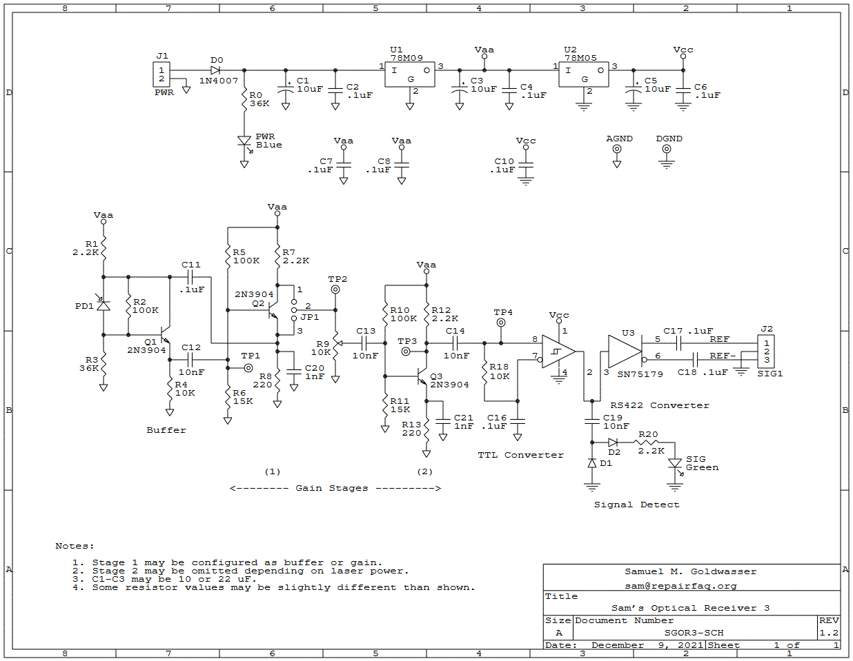
OR3 Version 1.2 Schematic
The graphic below shows the general appearance of the PCB with most of
the parts installed for the three levels of gain:

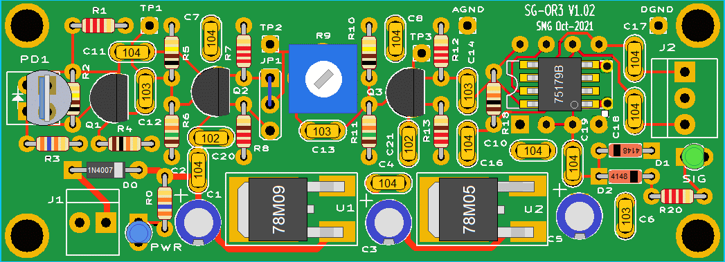
SG-OR3 PCB Version 1.02: Location of most Components with 75179B DIP (Left) and SOIC (Right)
Printing out the schematic and having it available for reference while
assembling the PCB may be helpful.
Assembly
As promised, here are the detailed "Heathkit™-style"
instructions for assembling the SG-OR3 V1.02 PCB.
All components are through-hole except for the voltage regulators (U1 and U1),
and except as noted in the detailed
assembly procedure, should seat flush on the
PCB. They shouldn't be suspended in mid-air swinging in the breeze. :)
The resistors in particular like to not stay flat on the PCB unless
their leads are bent at a steep angle.
Most components are identified on the silk-screen and with only a few
exceptions, the label won't be obscured when the part is installed.
A low power soldering iron with narrow tip and thin (e.g., #22 AWG) rosin-core
solder will be required. This is especially critical for the
SMT parts. DO NOT even think about attempting this without
suitable soldering equipment. It's well worth the investment. A Weller
soldering gun or propane torch will not work. :) Rosin core solder is also
essential. And while
I'm quite confident that you never make mistakes, a means of component removal
such as a de-soldering pump (e.g., a full size SoldaPullt™) will be
highly desirable. Screwing up component removal can easily ruin the PCB
and is not covered under the limited unlimited warranty. :-)
Proper soldering technique will be such that the exposed solder on each
pad should be shiny with a concave profile. It should not be a blob and
just needs to fill the hole. Solder is not glue.
Some excess solder doesn't hurt anything
but looks unprofessional. A 10X magnifier may come in handy for
inspection. Residual rosin can be cleaned off with
isopropyl alcohol or an environmentally-friendly electronic solvent.
However, leaving the rosin alone is also acceptable (if ugly).
Total assembly time should be well under 1 hour for someone proficient
in fine soldering. Cutting component leads to 1/4 to 3/8 inch before
installation will simplify soldering as the long leads won't be poking
you in your one good eye. :( :) Then trim flush after soldering.
Print out this document so each step can be checked off ( ) as it is completed.
The parts list below assumes populating with with
all components. Exceptions will be noted. Also note that if OR3 is used
near maximum gain to be able to detect a very low level optical input (<2
µW), it may need to be installed in a shielded box (not included).
- ( ) Confirm that all parts are present and undamaged:
- ( ) 1x blank SG-OR3 V1.02 PCB. Confirm the version on the
silkscreen. Inspect for plating or other defects.
- ( ) 3x 10 or 22 µF electrolytic capacitor.
- ( ) 8x 0.1 µF ceramic capacitor (marked 104).
- ( ) 4x 10 nF ceramic capacitor (marked 103).
- ( ) 2x 1 nF ceramic capacitor (marked 102).
- ( ) 2x 36K ohm 1/8 W resistor (orange-black-orange).
- ( ) 2x 10K ohm 1/8 W resistor (brown-black-orange).
- ( ) 3x 100K ohm 1/8 W resistor (brown-black-yellow).
- ( ) 2x 15K ohm 1/8 W resistor (brown-green-orange).
- ( ) 4x 2.2K ohm 1/8 W resistor (red-red-red).
- ( ) 2x 220 ohm 1/8 W resistor (red-red-brown).
- ( ) 1x 10K trim-pot (marked 103)
- ( ) 1x 78M09 IC regulator.
- ( ) 1x 78M05 IC regulator.
- ( ) 1x SN75179B IC RS422 receiver/driver.
- ( ) 1x photodiode.
- ( ) 1x green LED.
- ( ) 1x blue LED.
- ( ) 3x 2N3904 transistor.
- ( ) 1x 1N4007 or 1N4149 or similar diode.
- ( ) 2x 1N4148 or 1N4149 diode.
- ( ) 1x 2 pin header with shell and pins or screw terminal block.
- ( ) 1x 3 pin header with shell and pins or screw terminal block.
- ( ) 1x 2 pin male-to-female socket strip.
- ( ) 1x 8 pin DIP socket.
- ( ) 1x 3 pin jumper block and jumper.
- ( ) 1x ~1x1 inch piece of Circular Polarizer (CP) sheet. This can be
used as a Linear Polarizer (LP) as described below.
Inspect the parts closely, especially the (yellow) ceramic capacitors as
they may all appear physically identical. The labeling is TINY and easy
to read incorrectly. It's also easy to misread the itty-bitty 1/8th
watt resistor color bands.
In some cases, slighlty different values for resistors may be included
such as 30K in place of 36K, but these should be intuitively obvious. ;-)
If extra parts are found (typically resistors), the value(s) had changed and
I was too lazy to remove the old ones. ;-)
Testing of the LEDs inserted into the PCB but prior to soldering is
recommended. They are very fragile the leads
are stressed while soldering. Bend the leads
out at a small angle so the LED stays in place
and cut them short but DO NOT solder until thee LED has been
confirmed to work. Then without stressing the leads, solder quickly
and retest.
Double check the part value before soldering. Use a magnifying glass
if necessary. As they say in carpentry: "Measure twice and cut once.".
Even with proper desoldering equipment, removing a part without damage
to either the part or PCB can be dicey.
- ( ) Install U1 (LM78M09 voltage regulator). This is most easily done
by adding a tiny bit of solder to the lower-right pad and then holding
the chip in place while heating that leg on the IC. Then solder the
upper right leg, and finally the tab with just enough solder to form a
continuous bead along its length.
- ( ) Install U2 (LM78M05 voltage regulator) in a similar manner.
- ( ) Install J1 (2-pin header or screw terminal block). For the header,
the plastic tab faces toward the center of the PCB. For the terminal
block, the wire access holes face out.
- ( ) Install PWR (blue LED). The longer lead goes toward the center
of the PCB and the flat goes toward the edge. See note above with
respect to soldering LEDs.
- ( ) Install D0. (This used to be a 1N4007
but will be a 1N4149 going forward.) Pay attention to the polarity.
- ( ) Install R0 (36K ohms, brown-black-orange).
- ( ) Install C1, C3, C5 (10 µF). Note polarity: Positive is marked
on the PCB and is also the square pad. Negative on the capacitor is
the line.
- ( ) Install C2, C4, C6 (0.1 µF).
- ( ) Carefully inspect for solder and component lead shorts and unsoldered
leads. Correct as needed.
- ( ) Smoke test #1. :) Connect a source of 12 to 15 VDC to J1. Pay
attention to polarity. The blue LED should come on and the far right
legs of U1 and U2 should have voltages very close to +9 VDC and +5 VDC
on them, respectively.
- ( ) Install C7, C8, C10, C11, C17, C18 (0.1 µF).
- ( ) Install C12, C13, C14, C19 (10 nF).
- ( ) Install C20, C21 (1 nF).
- ( ) Install R1 (2.2K ohms, red-violet-red).
- ( ) Install R2, R5, R10 (100K ohms, brown-black-yellow).
- ( ) Install R3 (36K ohms, orange-black-orange)
- ( ) Install R4, R18 (10K ohms, brown-black-orange).
- ( ) Install R6, R11 (15K ohms, brown-green-orange).
- ( ) Install R7, R12 (2.2K ohms, red-red-red).
- ( ) Install R8, R13 (220 ohms, red-red-brown).
- ( ) Install R20 (1K ohms, brown-black-red).
- ( ) Install R9 (10K ohm trim-pot, labeled 103).
- ( ) Install D1, D2 (1N4148 or 1N4149 diode). Pay attention to polarity.
- ( ) Install SIG (green LED. The longer lead goes to the left
and the flat goes to the right. See note above with respect to
soldering LEDs.
- ( ) Install JP1 (3-pin jumper block). The jumper shold be placed on
the top position for high gain and bottom position for low gain. JP1
may be omitted and replaced with a jumper wire if the desired position
is known.
- ( ) Install Q1, Q2, Q3 (2N3904 transistor). Pay attention to the
outline on the PCB. These will not seat flush but 1/8-1/4" off the PCB.
- ( ) Install SKT2 (2 pin male-female
socket strip). Although the PD can be soldered, the use of the socket
strip is recommended as the photodiode is nearly as sensitive to failure
due to heat from soldering as the LEDs. Note that there are two possible
adjacent locations depending on the polarity of the PD. The one toward
the center of the PCB can be used with the face of the PD pointing away
from the PCB. Or the other one can be used if the PD is folded over.
The anode of the PDs included in the kit is
the left pin facing the front with its legs down.
- ( ) Prepare the photodiode. Cut a ~4x5 mm piece of the circular
polarizer (CP) sheet to attach to the front of the photodiode.
The CP sheet has protective film on both sides. Carefully peel it off.
One side of the sheet has adhesive to stick to the PD. Press it firmly
in place. The polarization axis is at 45 degrees
so it can be attached with the edges aligned with those of the PD. For
installation in the solder strip, the leads of the PD can be cut to a
length of ~1/8 inch.
In the trivial triviality department, the front face of the
PDs in the kits will have an "X" shaped rainbow
appearance due to the behavior of the Quarter WavePlate
on the back of the CP. Why might this be?
- ( ) Install J2 (3-pin header or screw terminal block). For the header,
the plastic tab faces toward the center of the PCB. For the terminal
block, the access holes face out.
- ( ) Install U3 (SN75179B). The following depends on whether a
DIP or SOIC package is in the kit:
DIP (through-hole) version:
- ( ) Install SKT1 (8 pin socket). Pay attention to orientation.
- ( ) Plug U3 (SN75179B) into the 8 pin socket. Pay attention to
notch or dot. Confirm that all pins are seated properly in the socket.
The SN75179B can be damaged if installed incorrectly.
SOIC (SMT) version:
- ( ) SOIC: Place the 75179B in position on the SMT pattern taking particular
care that the orientation is correct. Not only can the IC be damaged if
installed backwards, but removing and replacing it is likely to destroy it
entirely. In order to prevent it from dancing away when the soldering iron
approaches, stick it down with a tiny dab of adhesive or place something
on top of it to prevent it from moving until at least 2 pins are soldered.
- ( ) Solder the corner pins first. Use the tiniest amount of solder on
the soldering iron tip and just touch it to the ends of the pins. Then
solder the remaining pins. Check for solder bridges.
- ( ) Carefully inspect for solder and component lead shorts and unsoldered
leads correct as needed.
- ( ) Smoke test #2: Apply power. Nothing should smoke. ;-)
- ( ) Operational test: A varying source of light or a two frequency
laser with a split frequency of 3 MHz or less will be required. If a laser
isn't immediately available, an LED flashlight with adjustable brightness
may suffice as they usually use PWM to control brightness. (with a
flashlight, the SIG LED may not be that bright due to the low PWM
frequency.) An oscilloscope is highly desirable as well
since the SIG LED can only show that something is there but not what it
looks like. The signal could be from a local AM radio station! ;( :)
With no optical input, the Signal LED should be off if the Gain trim-pot
is not above around 1/2 max (with both gain stages populated).
But a human hand near the input introduce enough signal
to set it off, so move out of the way. Or consider the response to
your AC personality to be a sufficient confirmation that at least
most of the circuit works. ;-) With a laser or other signal
source, the LED should be on. Attaching the output to µMD1 or
µMD2 would be a confirming test.
OR3 as configured above has two gain options selectable by the jumper on JP1
which differ by approximately a factor of 10. The high gain setting with
the jumper in the upper position results in a usable response down to below
2 µ at 2 MHz but may be more prone to pickup of RFI. The low gain
setting with the jumper in the bottom position should be usable with beam
power above around 25 µW and should be quiet at any setting of the
gain trim-pot. One or both of the jumper settings should be satisfactory
for most applications. And OR3 has been tested from below 2 µW to above
1 mW without moving the jumper or adjusting the trim-pot.
However, where it is known that the beam power will be high or in an
electrically noisey environment, eliminating the second gain stage may
be useful. See OR3 Gain
Options which describes these in more detail.
BUT AGAIN, THERE IS USUALLY NO NEED TO USE ANYTHING BUT THE DEFAULT,
ABOVE.
OR3 consists of an impedance matching stage, 1 or 2 stages of amplification,
a differential-to-TTL converter, TTL-to-RS422 converter, and SIG LED driver
circuit as follows:
- The input (1st) stage is modeled loosely on that of the HP-10780 but using
a common 2N3904 BJT in place of the hard-to-find JFET. The 2N3904 is
remarkably capable for a 25 cent (or less) part, with a bandwidth of 250 MHz.
The only change to the circuit is that the BJT needs to be biased into the
conducting state (via R2). This stage acts as a buffer for the photodiode
which is a low current source. Its performance with the BJT and JFET appears
to be similar.
- The 2nd stage either provides a gain of approximately 10x or just
buffering depending on the position of the jumper, JP1. C11 provides
positive feedback to partially cancel the photodiode capacitance. Since
the feedback gain of the emitter follower is less than 1, it is
unconditionally stable.
- The 3rd stage (if present) provides up to another 10x gain, adjustable
using the trim-pot, R9.
- The signal at this point is analog but may be clipped depending on
the selected gain and (AC) optical input. The RS422 receiver portion of the
SN75179B acts as a differential-to-TTL converter. Its specs allow for
the input signal to exceed the normal operating range as long as the
current is limited, which it is in this case to less than 1/10th the
allowable value.
- The TTL output of the SN75179B is AC-coupled to a diode charge pump to
light the LED when an AC signal is present. (The simpler circuit
with a coupling capacitor and signal diode with reverse polarity
across the LED did not work likely due to the LED's capacitance/slow
response.)
- The TTL output also goes to the driver portion of the SN75179B which
provides the RS422 signal AC-coupled to the µMD or other measurement
device.
Troubleshooting? What troubleshooting? ;-) Check for solder bridges and
unsoldered leads, that the correct parts are installed, and for those with
polarity, that they in the right way around. The LEDs die easily
damaged from stress during soldering as noted above - at least twice!
So, if the Power or Signal LED doesn't light, it may just be a bad LED.
The most likely cause of low or no sensitivity is an incorrect resistor
value somewhere - it's easy to accidentally misread the color bands.
The parts are reliable, though the SN75179B may fail if
plugged in backwards or if the 5 V regulator isn't regulating.
Beyond this, an oscilloscope will be desirable to be able to trace the
signal. There are several strategically placed test-points for this purpose.
For friendly tech support, feel free to contact me via the link at the top of
this page. ;-)