
For contact info, please see the Sci.Electronics.Repair FAQ Email Links Page.
Copyright © 1994-2016
Reproduction of this document in whole or in part is permitted if both of the
following conditions are satisfied:
1. This notice is included in its entirety at the beginning.
All Rights Reserved
2. There is no charge except to cover the costs of copying.
DISCLAIMER
mLMA1 is not intended to replace a high performance stand-along SFPI
controller with oscilloscope display. That may come in the future. However,
for a quick check to determine if a laser is suitable for interferometery
or holography, its capabilities may suffice. And mLMA1
does provide features not present in any known instruments like
simultaneous display of longitudinal modes in SFPI and mode sweep format,
and for V3, a REF frequency readout.
Acknowledgement
Thanks to Jan Beck for getting me interested
in microcomputer development. If anyone had told me
six months ago that I'd be writing code for an Arduino-compatible
board - and enjoying it (sort of) - I would have suggested
they were certifiably nuts. ;-)
Links to his Web information may be found under
References.
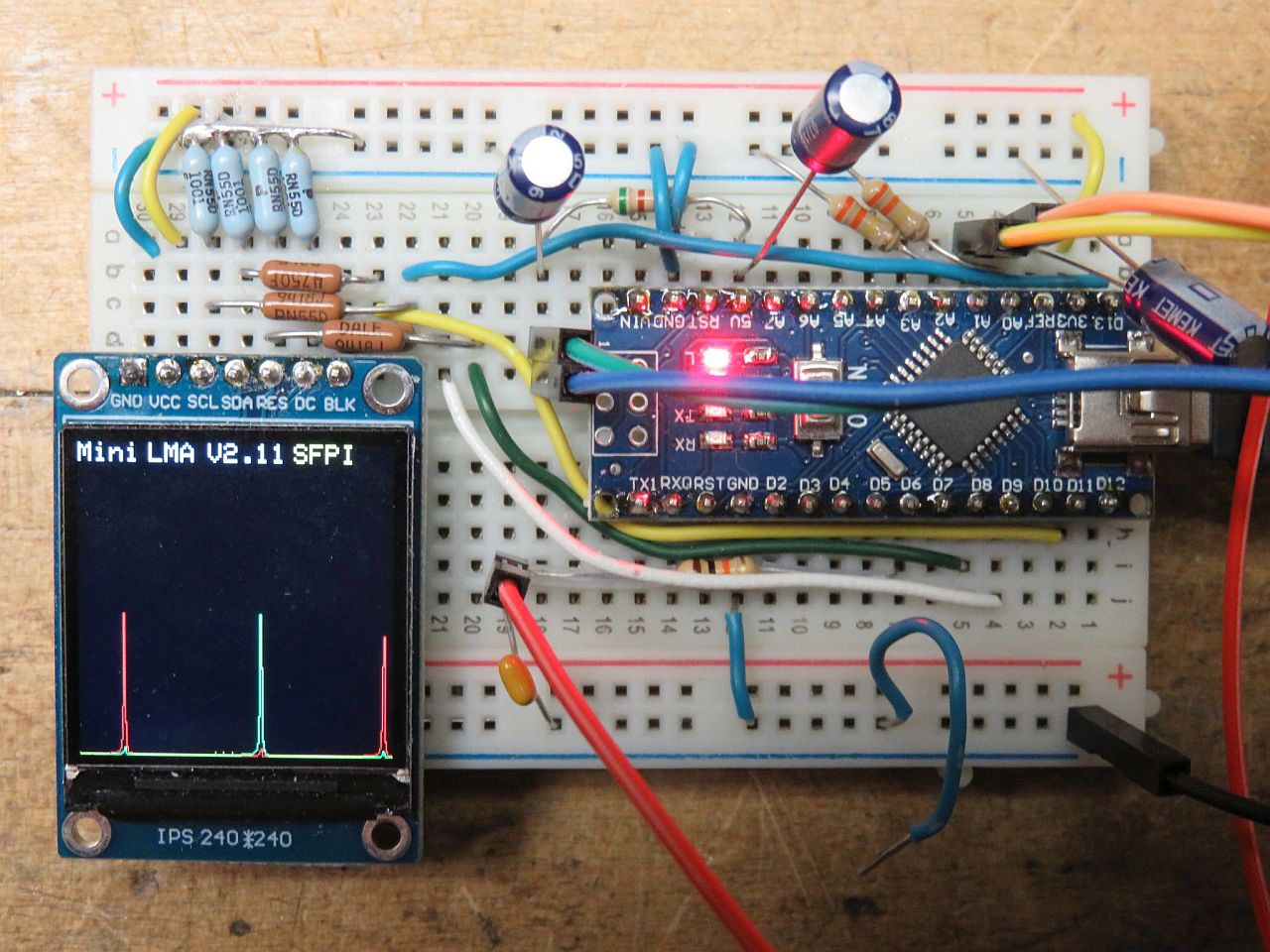
Mini Laser Mode Analyzer 1 (mLMA1) was originally intended as a proof of concept for implementing a Scanning Fabry Perot Interferometer (SFPI, also known as a laser spectrum analyzer) using any SFPI head compatible with low voltage PZT drive. But mLMA1 turned out so well that it could have practical value, especially where a compact low cost instrument is desired for basic checking of the mode behavior of lasers intended for applications like holography and interferometry. ;-) And then several other functions were added including a laser power meter, longitudinal mode display, and frequency counter. And it fully supports dual polarization inputs for all functions. Some of these capabilities do not have any known commercial counterparts. Though hopefully, creeping featurism syndrome beyond this will be largely avoided. :) At present, the hardware and firmware are mostly complete except for the addition of an antialiasinig filter for the SFPI display: If the finesse of the SFPI head is high, then peaks may be missed, or bounce up and down due to insufficient sampling. In other words, an SFPI head with low resolvance produces a nicer looking display. :) That may be remedies shortly, or at least eventually.
For use as an SFPI, mLMA1 replaces the normal ramp driver and oscilloscope by a compact almost zero-cost Arduino-based system with color LCD display. The accompanying "Mini" SFPI head constructed specifically for mLMA1 is just over 1x1x2 inches and includes the SFPI dual polarization detector as well as a beam sampler and longitudinal dual polarization detector So the entire setup could be fit in a pocket - really. :) Its entire parts cost - excluding that of the low voltage SFPI head - is under $10 using new and surplus parts, mostly from eBay. The SFPI head was built using Thorlabs 16 mm cage parts (around $100), the SFPI mirrors set I sell with my SFPI kits (~$50), and assorted odds and ends including surplus PBS cubes ($5-$10). This is designated the "Mini" SFPI head because, of course, there are also "Micro" and "Nano" versions which are even smaller. ;-)
A similar system with a higher performance processor and slightly higher resolution display would cost under $50, that may be Version 4. ;-) But the goal here really was to develop something usable as inexpensively as possible. Using a 600 MHz processor like the one in the Teensy 4.0 that would be twiddling it thumbs most of the time just seemed wasteful. :( :)
As can be seen based on the 1 inch-spaced holes on the optical breadboard, the head is around 2.5 inches overall. :) Additional descriptions of the mLMA1 hardware and optical head below.
V3 is virtually identical physically with a few pins being moved and upgraded firmware.
All functions support dual polarization displays:
The CHART function provides a moving graph of the longitudinal mode amplitudes in a format like a strip chart recorder with an end-to-end update time of around 2 minutes. The SCOPE function provides similar information in scope format (scan from left to right with an update time of as little as around 7 seconds).
All display functions can have dual polarization enabled whereby the P and S polarization orientations of the laser are displayed with different colors (assuing the use of an optical head or heads with dual polarization detectors). This doesn't impact the update rate/time very much.


As stated, these photos have been edited as it was not convenient to take photos for all the functions. Sorry, this will be updated eventually. But the general appearence is accurate. Details may vary.
The Laser power meter (POWER) displays the total power at an update rate of around 4 samples per second. (That can be speeded up.)

Data for CHART, SCOPE, and SFPI (in ASCII) may be saved to the host. For SCOPE, a value of 255 will be at the marker location (which is greater than the maximum valid data value of 192). POWER does not use trace buffers so the dump will be from whatever the previous function was. Data from COMBO will be from its last SFPI scan, but the data is at half amplitude. The displays for CHART and SCOPE will resume where they left off after the dump (but intervening data will be lost). Other functions will start fresh.
The system may be setup with an external trigger input so it can be synced to an experiment or high voltage ramp driver. When waiting for a trigger, it will display a marker in the upper right corner of the screen.
And just to show it's doing something if the data isn't changing, there is a single pixel to the right of the function text for all display modes that flashes as an "activity indicator".
The system described below implements all of these using the Atmega 328 Nano 3.0 PCB and a hand-full of discrete parts. SFPI scan rate, span, and offset; scan or sample rates for alll functions, and SFPI and MODE input gain can be adjusted via the "Three Button Interface described later. Trim-pots provide coarse adjustment of input sensitivity which should cover ranges sufficient for red HeNe lasers of at least 0.5 mW, and ramp amplitude (up to 9-10 V p-p) which should be enough to scan 2 FSRs or more using the typical $1 PZT beeper element. Together, these should be acceptable for a laser with an output power of 1 to 10 mW to display its longitudinal modes in real time. But a version using a previously implemented ramp driver and photodiode preamp PCB described in the Laser FAQ section:
While this won't replace a $5,000 instrument, it is more than adequate as-is for determining the basic health of a laser such as whether it is Single Longitudinal Mode (SLM). The display above shows the actual scan of the lognitudinal modes o a 5 mW red HeNe laser.
mLMA1 consists of 3 parts:
The Arduino-compatible Atmega 328 Nano 3.0 for mLMA1 provides the functions of both a low voltage ramp driver and Digital Storage Oscilloscope (DSO) using the 240x240 pixel color LCD display. The built-in ramp driver should work with home-built SFPI heads using PZT beeper elements as well as commercial ones like the SA-200 and others from Thorlabs that use low voltage drive. the ramp amplitude may be adjusted from 0 to almost 10 V p-p. For SPFI heads requiring a higher voltage ramp, a boost converter and driver transistor can be added.
The current implementation runs at over 10 scans per second using the 240x240 pixel IPS LCD. Since the display works like a DSO, this is way more than adequate since there is no flicker. Thus, even if scaled up to a large display in the future, the refresh rate should be acceptable. And of course, the $2 Nano is not exactly a stellar performer, so a higher performance microprocessor could be substituted if needed (though this LCD would have its own limitations due to the SPI data transfer rate).
A complete pocket-size SFPI based on mLMA1 could be built into a 1x2x4 inch case. :-)
This document provides a general descriptions of the mLMA1 hardware and firmware along with a wiring documentation, parts list, and construction guidelines.
The following assumes the use of the 43 mm RoC 99.4%R mirrors used in the SFPI kits.
There are two types of displays - chart recorder (CHART) and oscilloscope (SCOPE). When CHART is selected, the data scrolls from the right side of the screen. When SCOPE is selected, the data scans like an oscilloscope. :) The update rate for the two is the main difference: With dual polarization, for the chart recorder, it is up to around 16 points per second (full screen of around 15 seconds); for the scope, up to 50 or more points per second (full sweep of 5 seconds or less). These may be slowed via the TBI, by trivial changes to the firmware, or using external triggering. These are slightly faster without dual polarization.
Common to both:
The following two functions apply only to the DIP switch interface:
There are equivalent functions accessible when the TBI is active.
Specifications are subject to change without any prior notice. This is particularly true of the color schemes and it's 100 percent certainty that whatever photos are present in this document no longer reflect the colors in real life. ;-) (However, they are simple to customize in the firmware.)

The photos below show two types of dual polarization detector assemblies. The one on the left is installed behind the rear mirror for the SFPI including mounting holes for attaching to the rear cage plate. The beam comes in from the top (in the photo) and is split between the PD sitting beside the PBS cube and the one beneath it. Since the stack of the PD and PBS cube is thicker than a PD alone, spacers must be placed between the Perf. board and cage plate.
The one on the right would be used for the mode display of mLMA1 and is mounted along with the beam sampler between the front and middle cage plates. So its input is at a right angle to what is required for the SFPI. It is mounted to one side and a non-polarizing beam sampler directs a portion of the input beam into the PBS cube. Note that a simple glass plate is not very good for this if aligned with one of the principle axes as would be typical because it is highly anisotropic with respect to polarization - typically 4:1. But if oriented at 45 degrees to the principle axes along with the PBS, this issue would be eliminated. That could be tricky physically though.
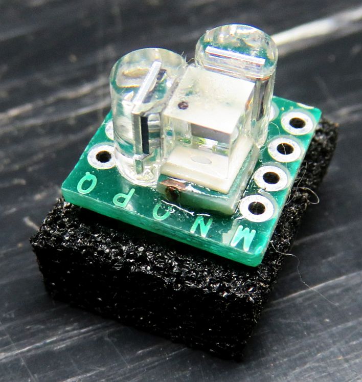

Note that the mirrors used here are known to be well behaved with respect to polarization even after hundreds or thousands of reflections. In other words, they do not affect the purity of the P and S polarized mode. This may not be true of dielectric mirrors in general many of which exhibit significant birefringence due to the technology used to create the coatings.

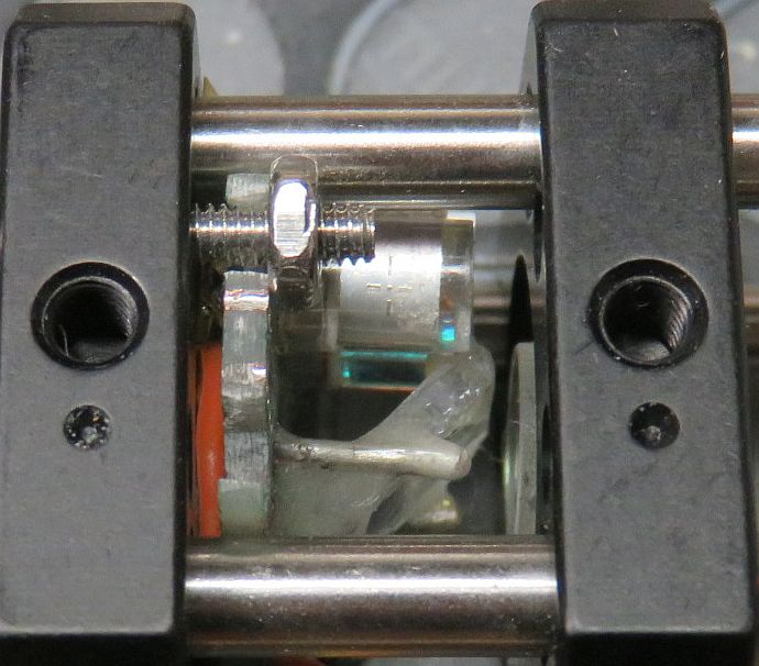
This shows what's in the optical head that was built except it doesn't have a frequency detector.
The 20 mm PZT has more than enough sensitivity, if anything too much as it picks up acoustic noise way too well. :( :)
A dual polarization SFPI detector assembly could be squeezed in behind the PZT with some spacers to increase in the space behind the rear mirror, though that was not installed for this version. But to add a dual polarization mode detector, a longer head would be necessary. But what fun would that be? ;-)
This was remarkably easy to set up for optimal mirror spacing by first sliding one of the cage plates on the rods for best display, and then alternately loosening the pair of set-screws on the left and right sides allowing for just enough movement to fine tune it.
Being so short, it nearly aligns itself to the laser. ;-)
While the resolution is not nearly as good as with the confocal spacing, it is still more than adequate to resolve the normal longitudinal modes (not Zeeman modes) of any common HeNe laser.
However, to implement the frequency counter required reassigning Atmega signal pins due to the convoluted relationships and limitations on the use of the internal Timers. And it was a close run thing at that. V3.xx firmware now supports both versions, but the first run of PCBs will not work with the frequency counter unless a few cuts and jumpers are done. Here is the summary - partially for reference so I don't forget it! It's really not important to a user:
The Atmega328P has 3 internal timers which have the following pin assignments and these cannot be changed:
  Name   Bits  PWM Pins  Clock Input Pins
------------------------------------------
 Timer0    8     D5,D6       D4 (T0)
 Timer1:  16    D9,D10       D5 (T1)
 Timer2:   8    D11,D3      D6 (TOSC1)
And since the SPI interface is used to drive the LCD, pins D9, D11, and D13 cannot be used for anything else because they, too, cannot be reassigned. The following juggling act appears to be the only one that will work:
  V2.xx  Unchgd  V3.xx
 AP  PP  AP  PP  AP  PP  Description
-----------------------------------------------------------------------------
         D2   5          SW1: Function_Select0, BT1: DOWN/OFF/BACKWARD
 D3   6          D4   7  SW2: Function_Select1, BT2: SELECT/TOGGLE
 D4   7          D7  10  SW3: Function_Select2, BT3: UP/ON/FORWARD
 D5   8          D3   6  Ramp-N: (moves from Timer 0 to Timer 2)
  ----           D5   8  REF frequency counter input (Timer1)
         D6   9          Ramp-P: (Timer 0)
 D7  10          D8  11  SW4: Dual_Polarization (ALL)
 D8  11         D16  21  SW5: Free_Run
         D9  12          LCD SPI DC: (Do not change)
        D10  13          SW6: Interpolation (CHART, SCOPE, SFPI, COMBO)
        D11  14          LCD SPI SDA (Do not change)
        D12  15          SW7: Filter/Average (ALL)
        D13  16          LCD SPI SCK (Do not change)
       V3.3  17          +3.3 V power
        REF  18          Analog reference voltage
        D17  22          SW8: Persistance (SFPI, COMBO/SFPI)
        D18  23          Sample_P: (POWER, CHART, SCOPE, COMBO/SCOPE)
        D19  24          LCD RES(ET) (Can reassign if desired)

         A0  19          SFPI_PMode (SFPI, COMBO/SFPI, 0-5V)
         A1  20          SFPI_SMode (SFPI, COMBO/SFPI, 0-5V)
         A6  25          MSweep_PMode (POWER, CHART, SCOPE, COMBO/SCOPE, 0-5V)
         A7  26          MSweep_SMode (POWER, CHART, SCOPE, COMBO/SCOPE, 0-5V)

        +5V  27          +5 VDC input or from on-board regulator

        VIN  30          Optional DC input (+7 to +12 VDC)
        GND 4,29         Ground/Common
 // set PCINT2 to trigger an interrupt on D2,D4,D7 state change
 PCMSK2 = (1 << PCINT18) | (1 << PCINT20) | (1 << PCINT23);
   // Set PWM frequency to ~63 kHz for Timers 0 and 2.
   // Timer0 prescaler setting affects millis() and delay() (~63x fast)

	TCCR0B = (TCCR0B & 0b11111000) | 1; No prescaling.
	TCCR2B = (TCCR2B & 0b11111000) | 1; No prescaling.
   // Initialize Timer1 for REF frequency counter and overflow interrupt
   // (refer to ATMega328.pdf chapter 16-bit counter1)

   TCCR1A = 0;  // reset timer/counter1 control register A
   TCCR1B = 0;  // reset timer/counter1 control register B
   TCNT1 = 0;   // Set counter value to 0
                // set timer/counter1 hardware as counter, counts events on
                // pin T1 (arduino pin D5), normal mode, wgm10 .. wgm13 = 0

   TCCR1B |= (_BV(CS10) | _BV(CS11) | _BV(CS12)); // Clk select external rising
TIMSK1 = TOIE1; // Set Timer1 overflow interrupt enable
The interrupt service routine would extend the 16 bit counter to 32 bits and then the frequency would be computed as the ratio of the difference between the last two interrupts (which would be very close to 65536 counts) and the system time difference between them. And that was implemented and worked. But it had the annoying characteristic that if the input frequency decreased below 100 kHz or so - or was zero as it would be periodically during warmup of a Zeeman laser - the display froze since there was insufficient information to update it.
So in the end, a much simpler scheme was implemented with no TIMER interrupts at all using a pair of TCNT1 reads separated by a fixed delay of 1 ms using delayMicroseconds(). It requires a couple lines of code to account for rollover of the 16 bit TCNT1 value (which would need to be done with the previous scheme as well) but other than that is more straightforward. The only downside is the 1 ms wasted time but an extra 1 ms once through the main loop is of little consequence.
However, The initial version required all interrupts to be disabled between the two reads of TCNT1 because the TIMER0 Overflow interrupt runs by default and is used by the delay(), millis(), and possibly other standard calls that deal with timing. Without disabling interrupts, the result was erratic and wrong. :( :) Not just slightly wrong, but super wrong. :( With the PWM frequency having been set to ~63 kHz, that meant an interrupt every ~16 µs which resulted in a useless overhead of something like 60 percent. For an input frequency of 1.88 MHz, the readout displayed around 3.06 MHz if the interrupts were not disabled because the 2 TCNT1 reads were ~10 µs too far apart. And that overhead was causing everything else to run slow as well.
To eliminate the 60 percent overhead not only between reads of TCN1 but for everything required replacing delay() with a custom subroutine called delay_Millis() which uses delayMicroseconds(), a standard call that simply uses a delay loop with a carefully selected number of clock cycles. Another benefit is that delay_Millis() isn't screwed up by the higher PWM frequency so it delays correctly in milliseconds.
And to fine tune the delay, the actual value sent to delayMicroseconds is 997 and a carefully selected kludge is added to fine tune the delay so that the readout is exactly 3.75 MHz for a 15.00000 MHz crystal divided by 4:
 ULTemp1 = TCNT1;        // Calculate frequency, gate time = 1 ms
 delayMicroseconds(997); // Actual delay runs with interrupts disabled
 UWTemp1 = 11111;        // Fine tuning delay kludge - adds 8 clock cycles :)
 ULTemp2 = TCNT1;
The actual assembly code for "UWTemp1 = 1;" is:
    26b4: 81 e0         ldi r24, 0x67 ; 103
    26b6: 90 e0         ldi r25, 0x2b ; 43
    26b8: 90 93 98 06   sts 0x0698, r25 ; 0x800698
    26bc: 80 93 97 06   sts 0x0697, r24 ; 0x800697
which takes 8 cycles. (One cycle is 62.5 ns for the Atmeag 328.) Whatever works. :) The funny value of 11111 is an attempt to assure that a clever compiler optimizer won't consider it a value that can be optimized out. :) Serious software engineers are probably rolling over in their graves, but so be it. ;-)
For comparizon, here are the execution times for values of 0 or a constant k not equal to 0 for an 8 bit byte, 16 bit word, and 32 bit long word:
    C Code      #bits   Cycles
 ------------------------------
  UBTemp1 = 0;     8     2-4
  UWTemp1 = 0;    16     4-8
  ULTemp1 = 0;    32     8-16
  UBTemp1 = k;     8      4
  UWTemp1 = k;    16     6-8
  ULTemp1 = k;    32    10-16
The number of cycles must be a multiple of 2. "0" may be a special case because it appears as though the compiler trys to keep r1 loaded with 0 so it can be used where 0s are required. The range of the number of cycles depends on (1) whether 0 is already in r1 and (2) whether the compiler realizes that 0 can be generated without loading it with an immediate operand using a register instruction such as XOR (eor r1, r1) for example. The funny value for k in the fine tuning delay will assure that it's always 8 cycles since both bytes of k will need to be loaded. The tuning granularity is thus 125 ns (2 cycles) or 1 part in 8,000 for the 1 ms total delay.
In fact, the only active interrupt of any kind is now for the buttons. And with all other interrupts disabled, functions like SFPI run very noticeably faster. ;-)
Below is the compiler-generated Atmega328 assembly code for the TIMER0_OVF Interrupt Service Routine (ISR) as determined from the <PROJECTMAME>.elf file found at C:\<BUILDPATH>\<BUILD>\<'PROJECTNAME> using the command (via the CMD Prompt from within that directory): <ARDUINOPATH>\avr-objdump.exe -d <BUILDPATH>\<PROJECTNAME>.elf > <PROJECTNAME>.asm. (The "<>" means replace with the actual path dropping the "<>".) In my case, "BUILDPATH" was C:\users\sam\AppData\Local\Temp\ and "BUILD" was build-6221dfb7-d8c9-47af-87f7-e2fa0fc3109e\ . (Each build-number will be unique.) "ARDUINOPATH" was D:\Program Files\Arduino-1.8.10\hardware\tools\avr\bin\ . So the actual command when executed from the BUILD directory was: C:\users\sam\AppData\Local\Temp\build-6221dfb7-d8c9-47af-87f7-e2fa0fc3109e\ D:\Program Files\Arduino-1.8.10\hardware\tools\avr\bin\avr-objdump -d mLMA1_fw_V2.82o.elf > mLMA1_fw_V2.82o.asm .
The ISR originates in the UECIDE wiring.c library for the Atmega 328 at \USER\AppData\Local\UECIDE\cores\arduino\arduino which is the same as the Arduino version at \Program Files\Arduino-1.8.10\hardware\arduino\avr\cores\arduino\wiring.c .
 Bytes+  Program  Instruction
 Cycles  Counter     Words     Assembly Code      ; Comments/Annotation
------------------------------------------------------------------------------
     00005daa <__vector_16>:

  2+2     5daa:      1f 92        push  r1
  2+2     5dac:      0f 92        push  r0
  2+1     5dae:      0f b6        in  r0, 0x3f    ; 63
  2+2     5db0:      0f 92        push  r0
  2+1     5db2:      11 24        eor r1, r1
  2+2     5db4:      2f 93        push  r18
  2+2     5db6:      3f 93        push  r19
  2+2     5db8:      8f 93        push  r24
  2+2     5dba:      9f 93        push  r25
  2+2     5dbc:      af 93        push  r26
  2+2     5dbe:      bf 93        push  r27
  4+1     5dc0:      80 91 66 07  lds r24, 0x0766 ; 0x800766
  4+1     5dc4:      90 91 67 07  lds r25, 0x0767 ; 0x800767
  4+1     5dc8:      a0 91 68 07  lds r26, 0x0768 ; 0x800768
  4+1     5dcc:      b0 91 69 07  lds r27, 0x0769 ; 0x800769
  4+1     5dd0:      30 91 65 07  lds r19, 0x0765 ; 0x800765
  2+1     5dd4:      23 e0        ldi r18, 0x03   ; 3
  2+1     5dd6:      23 0f        add r18, r19
  2+1     5dd8:      2d 37        cpi r18, 0x7D   ; 125
  2+1 (1) 5dda:      20 f4        brcc  .+8       ; 0x5de4 <__vector_16+0x3a>
  2+1     5ddc:      01 96        adiw  r24, 0x01 ; 1
  2+1     5dde:      a1 1d        adc r26, r1
  2+1     5de0:      b1 1d        adc r27, r1
  2+2     5de2:      05 c0        rjmp  .+10      ; 0x5dee <__vector_16+0x44>
  2+1     5de4:      26 e8        ldi r18, 0x86   ; 134
  2+1     5de6:      23 0f        add r18, r19
  2+1     5de8:      02 96        adiw  r24, 0x02 ; 2
  2+1     5dea:      a1 1d        adc r26, r1
  2+1     5dec:      b1 1d        adc r27, r1
  4+2     5dee:      20 93 65 07  sts 0x0765, r18 ; 0x800765
  4+2     5df2:      80 93 66 07  sts 0x0766, r24 ; 0x800766
  4+2     5df6:      90 93 67 07  sts 0x0767, r25 ; 0x800767
  4+2     5dfa:      a0 93 68 07  sts 0x0768, r26 ; 0x800768
  4+2     5dfe:      b0 93 69 07  sts 0x0769, r27 ; 0x800769
  4+1     5e02:      80 91 6a 07  lds r24, 0x076A ; 0x80076a
  4+1     5e06:      90 91 6b 07  lds r25, 0x076B ; 0x80076b
  4+1     5e0a:      a0 91 6c 07  lds r26, 0x076C ; 0x80076c
  4+1     5e0e:      b0 91 6d 07  lds r27, 0x076D ; 0x80076d
  2+1     5e12:      01 96        adiw  r24, 0x01 ; 1
  2+1     5e14:      a1 1d        adc r26, r1
  2+1     5e16:      b1 1d        adc r27, r1
  4+2     5e18:      80 93 6a 07  sts 0x076A, r24 ; 0x80076a
  4+2     5e1c:      90 93 6b 07  sts 0x076B, r25 ; 0x80076b
  4+2     5e20:      a0 93 6c 07  sts 0x076C, r26 ; 0x80076c
  4+2     5e24:      b0 93 6d 07  sts 0x076D, r27 ; 0x80076d
  2+2     5e28:      bf 91        pop r27
  2+2     5e2a:      af 91        pop r26
  2+2     5e2c:      9f 91        pop r25
  2+2     5e2e:      8f 91        pop r24
  2+2     5e30:      3f 91        pop r19
  2+2     5e32:      2f 91        pop r18
  2+2     5e34:      0f 90        pop r0
  2+2     5e36:      0f be        out 0x3f, r0    ; 63
  2+2     5e38:      0f 90        pop r0
  2+2     5e3a:      1f 90        pop r1
  2+4 (2) 5e3c:      18 95        reti
Bytes is the size of the intruction and Cycles is the execution time But apperently, only Bytes matters most of the time due to overlapped fetch and excuate from different memories. This code would then be approximately 148 cycles which is close to the value estimated based on the error in the frequency counter readout.
Notes:
The length and complexity of the ISR is in part due to the need to handle 32 bit words for the counts on an 8 bit CPU. But even so, it seems longer than it needs to be.
The latest firmware is fully functional for the frequency counter (FC) input which is enabled by changing uncommenting the #define FC statment.
The range for frequency measurement is from 0.000 MHz to 6.400 MHz. The high limit is due to issues with how the counting synchonization interacts with the 16 MHz Atmega system clock. From the Atmega manual:
"Each half period of the external clock applied must be longer than one system clock cycle to ensure correct sampling. The external clock must be guaranteed to have less than half the system clock frequency given a 50/50% duty cycle. Since the edge detector uses sampling, the maximum frequency of an external clock it can detect is half the sampling frequency (Nyquist sampling theorem). However, due to variation of the system clock frequency and duty cycle caused by oscillator source (crystal, resonator, and capacitors) tolerances, it is recommended to limit the maximum frequency of an external clock source to less than fclk_IO/2.5."
fclk_IO is the same as the CPU clock - 16 MHz so the recommendation is 6.4 MHz max. From 4.0 MHz to 6.4 MHz, the display color will change to show that there could be issues with accuracy if the input waveform is highly asymmetric. Above 6.4 MHz, the display will show "-.---" in RED. If you insist on living dangerously, it's easy to change these thresholds in the firmware but be forewarned of aliasing. ;-)
The most convenient input would be from an HP optical receiver, or the output from the REF output of a 5501B or 5517 laser if that's what's being tested (though level shifter may still be required depending on whether that output has TTL levels or is transformer or capacitor coupled). However, since the optical power available can be reasonably high (10s of µW) with a suitable beam sampler, a relatively simple optical receiver circuit like the one below can be used. (Click on the graphic for the PDF version.)

The photodiode part number is what's used in the Teletrac laser but any small-area silicon photodiode will work just as well. And the 2N2222s can be replaced by 2N3904s or other similar general purpose NPN transistor, though the 2N5210 should have better performance. Using a 10 percent beam sampler and linear polarizer at 45 degrees to the polarization axes should result in satisfactory performance. Note that if a simple glass plate is tilted at 45 degrees in the X or Y axis and used as a beam sampler, the result will be highly unequal signal amplitudes for the two frequency components. This is because 45 degrees is fairly close to the Brewster angle of 57 degrees and one component ends up being roughly 4 times the amplitude of the other. A polarization isotropic beam sampler can be used like the ones found in HP/Agilent/Keysight lasers, or the beam sampler can be rotated by 45 degrees about the optical axis which would make mounting interesting.
The new version of the PCB supports the frequency counter and includes a transistor buffer that can be configured so the signal can come directly from an HP/Agilent/Keysight laser or opticsl receiver, or be almost anything else - capacitor coupled, transformer coupled, or direct TTL, CMOS, or ECL levels, etc.


Note: V2 and V3 here should not be confused with the firmware version, which can be anything. ;-) And V3.xx firmware supports both via a #define statement.
The only wiring differences between V2 and V3 are for Function_Select1 and Function_Select2, Ramp-N, Dual_Polarization, Free-Run, and the addiion of the REF_Input for the frequency counter. So, modifying the V2 PCB for V3 would be fairly simple. However, the V3 PCB will also have a transistor buffer that can be configured for AC or DC coupling and signal level (not shown on the diagram above). A header may be installed in the location of the unused 5 pins of the DIP switch for possible additional I/O signals if desired. The V3 PCB will have an adjacent ground pad that can be used as the return for the signals.
However, V3 also has space for several components that may be configured in various ways to accept the frequency counter input (REF) as TTL, AC, etc. The values shown are just guesses - they will be need to be selected based on the signal type and amplitude. If the frequency counter is not being used, these can be ignored.
For the original prototype, most of the half dozen connections on the breadboard were made with the electronic parts themselves or bits of excess wire cut from their leads. But there will be a need for a few insulated jumpers which should use #22-#24 AWG solid hookup wire stripped to fit in the holes. Thinner wire may not make secure connections. The DIP switch and buttons were soldered to their own small Perf. boards and then attached to the breadboard with header strips. However, solderless breadboards, especially if previously used, can be unreliable so this method of assembly is not recommended.
Power for the IPS 240x240 pixel full color LCD is 3.3 VDC. Its signal pins may not be 5 V-tolerant so it is critical to use voltage dividers for the 4 signals so that they never go above 3.3 V. Assure that these connections are secure as even a momentary transgression may have bad effects. Also, the pinout for the LCD may differ depending on where it was purchased. Especially important are VCC and GND, which may be swapped. Connecting it with reverse polarity even for an instant will likely damage or destroy the device. (Don't ask me how I know.) So for testing, do not just pull one display out and poke another one in without checking the pin labels!
For just testing the ST7789 SPI LCD, only the following is required:

The resistor values for the level shifter (here and for the full mLMA1) are not critical as long as they are approximately in the ratio of 2:1. So 1K with 470 to 510 ohms should be fine. But they shouldn't be much smaller (due to drive considerations) and if too large, there may be problems with the frequency response. Under some undetermined conditions, a 100 pF capacitor between D11 and GND is needed to prevent erratic behavior. There is probably a race condition in the ST7789 library SPI timing. More on this under "Troubleshooting", below.
If you have an mLMA1 PCB, it can be used to test the LCD before fully populating it. Or the circuit, above, can be built on a prototyping board or solderless breadboard. The level shifter resistors are all in one block under the LCD. R7-R10 are ~500 ohm; R11-R14 are ~1K ohm. See Testing the ST7789 LCD using the Atmega 328P Nano 3.0 and Arduino IDE for details.
CAUTION: Make to use the proper libraries are used for each IDE. Due to what may be a bug in the Arduino complier, the bootloader was damaged or erased when using the Arduino library with the Arduino IDE. Go figure. Or perhaps I was hallucinating. :( :) Restoring the bootloader is straightforward but does require the use of the USBAsp. See the section: Uploading firmware or burning the bootloader using a USBasp ISP.
This is a variation of a number of similar sketches found on the Web that can exercise the LCD without requiring any hardware much beyond the Nano and a few resistors as described above. The normal mLMA1 firmware may also be used. Either of these can also be used to determine if a specific LCD comes up in normal or 8 color mode (see below).
Electronic parts list for mLMA1-V2 using V2.0 or V3.0 PCB
 Qty Description                    Comments
-------------------------------------------------------------------------------
 ^1  Atmega 328P NANO 3.0           Arduino board

 ^1  ST7789 240x240 pixel IPS LCD   SPI 1 inch Color LCD display.  Note: For
                                     an unknown reason, some LCDs only display
                                     8 colors rather than the full range.
                                     The mLMA color scheme is designed so this
                                     doesn't matter much, but it's just not as
                                     cool.  It is probably an initialization
                                     bug deep in the library code.  Sorry, I'm
                                     not going there. ;-)

                                     There is a predefined color scheme that
                                     is slight better with these LCS, see
                                     #define option in the firmware.

 ^1  mLMA1 V2.0 PCB                 "#define FC" must be commented out.
 ^1  mLMA1 V3.0 PCB                 "#define FC" must NOT be commented out..

 ^1  6x8 cm Perf. board             If not using PCB

 ^1  Socket, 30 pin 0.6 inch DIP    For Atmega 328P NANO 3.0
 ^1  Socket, 7 pin SIP              For LCD

  1  Super bright LED, 3 mm         Sample indicator
  1  Super bright LED, 3 mm         Ramp indicator

  2  Resistor, 10K ohm, 1/4 W       Current limiting for LEDs

 ^4  Resistor, 470-510 ohm, 1/4 W   5V-3.3V level conversion
 ^4  Resistor, 1K ohm, 1/4 W        5V-3.3V level conversion

  2  Resistor, 15K ohm, 1/4W        Ramp filter

  1  Resistor, 220-360 ohm, 1/4 W   Photodiode protection

  1  Resistor, 1K ohm, 1/4 W        External Trigger input

  2  Trim-pot, 1M ohm               SFPI P and S gain
  2  Trim-pot, 100K ohm             MODE P and S gain

  1  Trim-pot, 1M ohm               Ramp amplitude

  2  Capacitor, 0.1 µF              Ramp filter

  2  Capacitor, 100 pF              SFPI P and S PD filter (optional)
  2  Capacitor, 1 nF                MODE P and S PD filter (optional)

 ^2  Capacitor, 22 µF               5V and 3.3V bypass
  2  Capacitor, 22 µF               REF and PD bypass

 ^1  Capacitor, 100 pF              D11/SDA kludge +

  1  DIP switch, 8 position         "Piano key" style function/option select *

  3  Tactile switch                 Three button interface
^ These are the required parts for the LCD test version ONLY. LEDs optional.
* The DIP switch is no longer really needed with the three button interface being fully functional and providing more capability. And not populating the DIP switch makes several pins available for other functions that may be added by the mLMA Creeping Featurism Department. :)
+ This capacitor may be needed to avoid data errors to the LCD resulting in it freezing or going blank, particularly if the +5V is marginal as it might be if powered via USB. There may be a bug in the SPI code or hardware making the SCK-SDA timing too critical. I would give an "F" for any student design like this but so be it. :( :) Locating the bug is above my pay grade. ;-)
Additional electronic parts for V3.0 PCB with frequency counter
The actual values for these components may depend on signal characteristics.
 Qty Description                    Comments
------------------------------------------------------------
  1  NPN transistor, 2N5210,        Frequency counter signal buffer
      2N3904, 2N2222, etc.

  1  Diode, 1N4148                  Input network

  2  Capacitor, 0.1 µF              Input AC coupling

  1  Resistor, 100 ohm, 1/4 W       Series input
  2  Resistor, 1K ohm, 1/4 W        Input network
Connectors and hardware
 Qty Description                    Comments
-------------------------------------------------------------------------------
  1  Screw terminal block or        5V Power
      Header, 2 pin
                                    If header, a mating 2 pin shell and
                                    2 socket pins will be included.

  1  Screw terminal block or        5V Power
      Header, 3 pin
                                    If header, a mating 3 pin shell and
                                    3 socket pins will be included.

  1  Screw terminal block or        SFPI input and ramp drive connector
      Header, 5 pin
                                    If header, a mating 5 pin shell and
                                    5 socket pins will be included.

  1  Screw terminal block or        SFPI input and ramp drive connector
      Header, 4 pin
                                    If header, a mating 4 pin shell and
                                    4 socket pins will be included.

                                    Aux input connector

  4  M3-10mm machine screw          Feet for prototyping board or PCB
  4  M3 nut                         For feet

  2  M2-18mm machine screw          LCD mounting
  6  M2 nut                         For LCD mounting
The 10K ohm value for the LED current limiting resistors are not typos. These are ultra bright 3 mm LEDs. Look for LEDs with a voltage drop of ~3 V. Even 10K is really too low. :) 25K or more would still result in adequate brightness. All white and blue LEDs are ultra-bright; 3 mm water clear green is usually ultra-bright, but confirm when buying. Most other colors are not, at least as of 2020.
Dual polarization optical head parts list
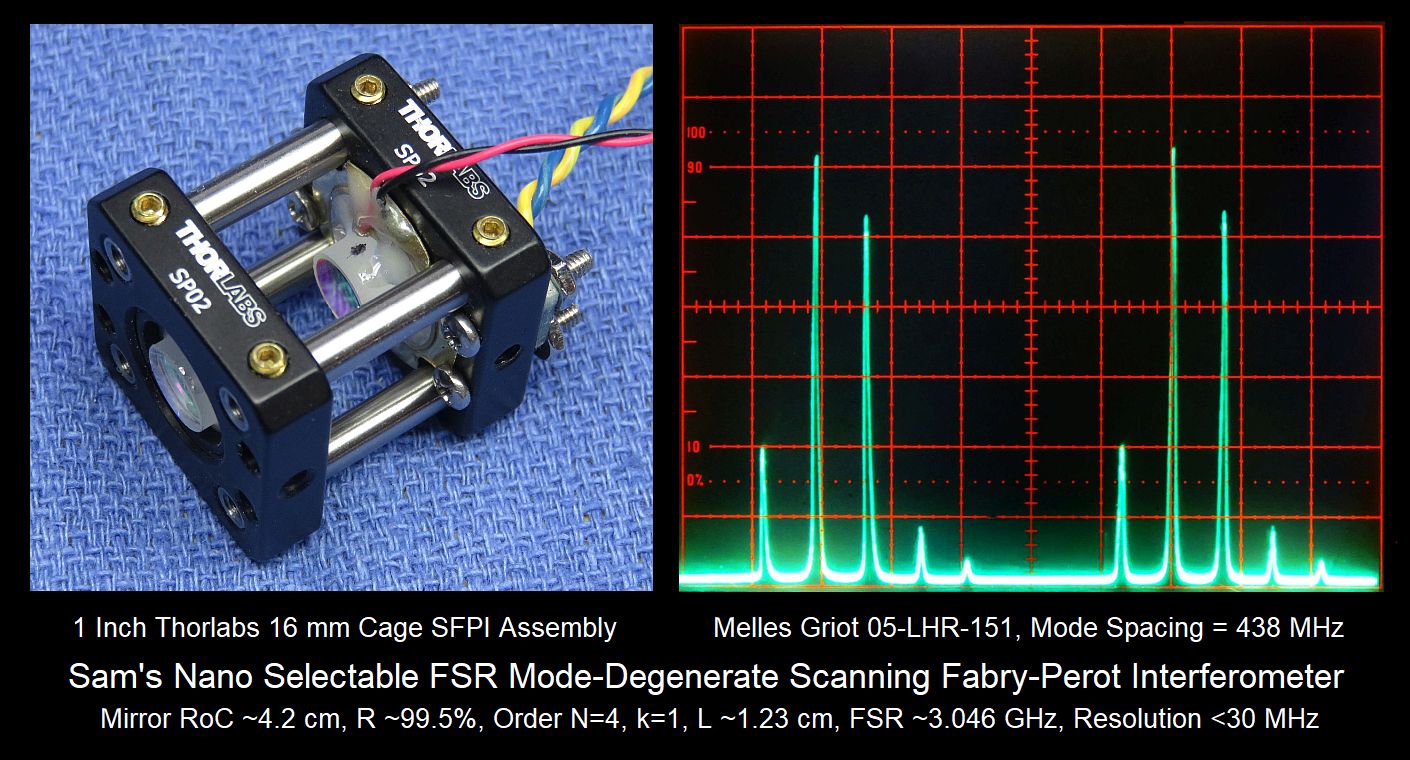
The Thorlabs parts are for the Mini SFPI head, approximately with dimensions just over 1x1x2 inches. For the Micro or Nano, change the cage rods to SR1.5-P4 or SR1-P4, respectively.
 Qty Description                    Comments
-------------------------------------------------------------------------------
  3  Thorlabs SP02                  Compact Cage Plate with SM05 Thread
  1  Thorlabs SR2-P4                4 mm Compact Cage Rod, 2.0 inch, 4 Pack
  1  Thorlabs LMRA8                 8 mm Adapter for LMR05 for front mirror

  1  Lens, ~50 mm FL, ~12.5 mm D    Surplusshed L14148 or Thorlabs LA1213
  2  SFPI mirrors, matched          42 mm RoC, 7.75 mm D, 99.5%@633 nm, S2 AR
  1  PZT element, 20 mm             Digikey 490-7712-ND with 4-5 mm hole added

  2  PBS cube, 4x4x4 mm, 633 nm     For dual polarization detectors
  4  Photodiode, 2.5x2.5 mm         OSRAM SFH206K for above
  1  Beam sampler, 6 mm, 15-20%     Use at 45 degrees for MODE detector

  1  Prototyping board, ~2.5x5 cm   Cut into two pieces for PBSs, PDs, and BS

  8  M2-12 machine screw            PZT and dual polarization detector mounts
 12  M2 nut                         For above.
The SR2 2" cage rods assume a mirror spacing of 1/2 the RoC (N/k=3/1) or less. For the confocal spacing with the full RoC, switch to SR3 3" or SR4 4" rods. For the Micro SFPI head, the mirror spacing is limited to N/k=4/1 but but there is still room to squeeze in the dual polarization detectors for both the SFPI and Mode displays. The Nano SFPI head may still be used with N/k=4/1 but without the Mode detector.
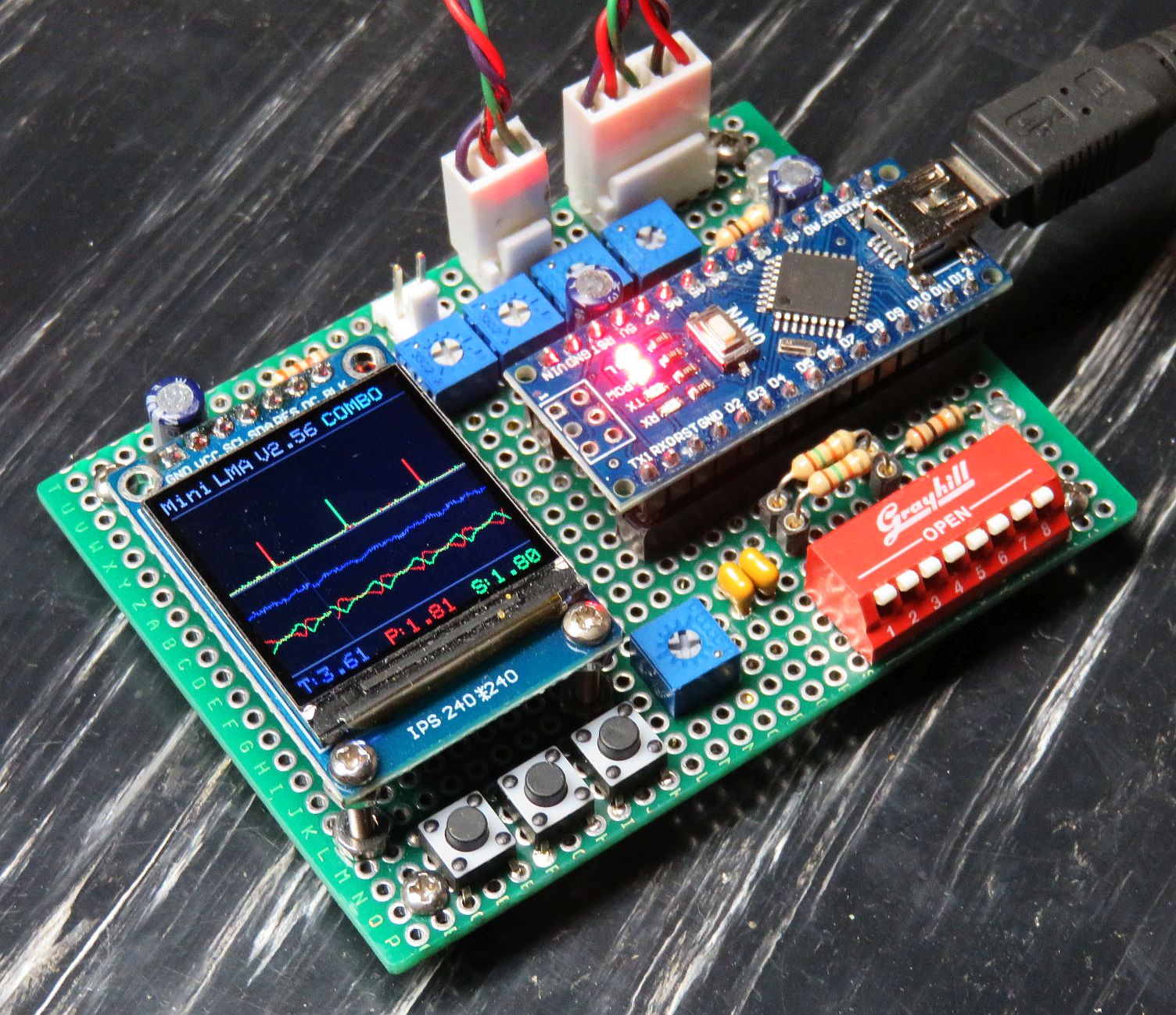
The Perf. board is around 6x8 cm with sockets for the Atmega and LCD, and will have all the components in the wiring diagram EXCEPT for the DC-DC and MHV-PZT driver. Also includes the buttons for the three button interface. The PCB will be very similar.
This photo of mLMA1 running in the COMBO function has not bee doctored or mangled in any way except to remove some dust specks. :) The design is identical to what's shown in the wiring diagram and parts list. The 5V to 3.3V conversion resistors are under the LCD.
The complete schematics may be found as PDFs at at Mini Laser Mode Analyzer V2.0 Schematic and Mini Laser Mode Analyzer V3.0 Schematic.


The dimensions are just over 8 x 6 cm (3.2 x 2.4 inches), similar to the prototype.
Of course there's already two ECOs for the PCB:


The mLMA1-V3.0 PCB which includes the frequency counter input should be the one currently shipping.
  Arduino  Physical
    Pin      Pin     Function
-------------------------------------------------------------------------------
     D2       5      SW1: Function_Select0 (Function_Select210: DLHLD=0,
     D3       6      SW2: Function_Select1  POWER=1, CHART=2, SCOPE=3, SFPI=4,
     D4       7      SW3: Function_Select2  SFPI=4, COMBO=5, HOLD1=6, HOLD2=7)

     D2       5      BT1: DOWN/BACKWARD    (Three Button Interface if
     D3       6      BT2: SELECT            Function_Select210==7 at startup)
     D4       7      BT3: UP/FORWARD

     D5       8      Ramp-N - Complement of D6 (SFPI, COMBO/SFPI)
     D6       9      Ramp-P - PWM of scan ramp (SFPI, COMBO/SFPI)
     D7      10      SW4: Dual_Polarization (ALL)
     D8      11      SW5: Free_Run (ALL)
     D9      12      LCD SPI DC (Do not change)
    D10      13      SW6: Interpolation (CHART, SCOPE, SFPI, COMBO)
    D11      14      LCD SPI SDA (Do not change)
    D12      15      SW7: Filter/Average (ALL)

    D13      16      LCD SPI SCK (Do not change)
    V3.3     17      +3.3 V power
    REF      18      Analog reference voltage
    D16      21      DSpare16
    D17      22      Persistance (not on Rev 1 PCB)
    D18      23      Sample_P (POWER, CHART, SCOPE, COMBO/CHART/SCOPE)
    D19      24      LCD RES(ET) (Can reassign if desired)

     A0      19      SFPI_PMode input (SFPI only), 0 to 5V
     A1      20      SFPI_SMode input (SFPI only), 0 to 5V
     A2      21      ASpare2
     A3      22      (D17)
     A4      23      (D18)
     A5      24      (D19)
     A6      25      MSweep_PMode input (POWER, CHART, SCOPE), 0 to 5V
     A7      26      MSweep_SMode input (POWER, CHART, SCOPE), 0 to 5V
    +5V      27      +5 VDC input or from on-board regulator

    VIN      30      Optional DC input (+7 to +12 VDC)
    GND     4,29     Ground/Common
D0 and D1 are used by the serial port for startup information and for the DLHLD function. If there is ever a way to upload data, they would be required.
The COMBO function splits the screen into two equal sections vertically and uses the SFPI inputs for the SFPI (upper) display and Mode Sweep inputs for the SCOPE (lower) display.
CAUTION: The Nano 3.0 can take +12 VDC on VIN since it has an on-board 5 V regulator. But apparently there can be problems when connecting to USB as I found out. Inadvertent ground loops (or something) can result in erasing its brain or damaging the USB chip. Exactly why this occurred is still not clear. The NANO was connected to USB and then the 12 V adapter was plugged in, at which point the USB dropped out, never to be heard from again with this board. The regulated wall adapter was on the same circuit and isolated in any case, so it should not have caused problems. The Atmega microprocessor is still running something so it's not totally dead, thus the suspicion that the problem is the USB chip. But I've been unable to change it so far, even with a programmer. On another board, the USB is alive but firmware cannot be downloaded - either the Atmega chip is dead or the boot loader code was damaged. Therefore, it is recommended that only the USB on a PC or laptop, a USB wall adapter, USB backup battery, or 5 V power supply be used.
  Mini Laser Mode Analyzer Version: 2.54

  Display Initialized

  SFPI Antialiasing Filter Kernal, Span: 1.00

  1.00
  0.83
  0.46
  ....

  Running
The numbers are the weights for the FIR filter from 0 to 31 (and by symmetry, from 0 to -31.) They are computed by: sin(x*Span)/(x*Span) normalized to a maximum of +127/128 with an offset of 128. Changing the value of Span in the firmware can be used to adjust the filter bandwidth. The antialiasing filter is still a works in progress.
In addition, the DLHLD function may be used to dump the contents of the trace buffers for for the function active at the time of the dump (CHART, SCOPE, SFPI, or COMBO/SFPI).
The buttons are: B1: DOWN/OFF/BACKWARD, B2: SELECT/TOGGLE, B3: UP/ON/FORWARD.
In all cases, selections for each of the buttons are shown, replacing the banner in the top-left portion of the display while the buttons are in use (so as not to interfere with the selected function, which continues to run except in some cases while parameters are being adjusted).
Top level: B1 and B3 cycle between POWER, CHART, SCOPE, SFPI, and COMBO functions, and SETTINGS and DEFAULTS.
For the functions, pressing B1 switches to the highlighted function and goes to the second level.
For SETTINGS and DEFAULTS the previous function continues to run.
Second level: The effect of B1 (moves to the left) and B3 (moves to the right) depends on which function is active and cycles among:
(The highlight function and EXIT are essentially equivalent at this level but EXIT is included so there is no doubt how to get out of it!) The RATE parameters are function-specific and their actual effect may differ. SPAN and OFFSET are for the SFPI sweep. KERNAL is a number from 1 to 10 that determines the width of the windowed sin(x)/x antialiasing filter kernal. A value of 0 disables the antialiasing filter. (FILTER must also be enabled under UTILITIES.)
Except for RATE, parameters for COMBO are handled by SFPI and SCOPE. RATE for COMBO adds an additional way to slow things down further, should there be some need to do so.
And for the others:
B2 selects the value to adjust or toggle and goes to third level (except for the active function or EXIT (which result in the same actiion - to go back to first level), or where an option has its own action (like the toggle for dual_polarization or interpolation).
Third level:
B1/B3 adjusts value up/down or toggles value on/off. Using RATE as an example, the current value of the parameter will be displayed momentarily and then the button navigation display will look something like the following:
- RATE +
Actions take effect when the next sample or scan occurs. For the adjustments, + and - denote the effect of B1 and B3. A momentary press of B1 or B3 will cause the value to decrement or increment by 1 if within the allowable range. If at one end, either + or - will be missing and it will just stay there, as well as the current value appearing momentarily in place of the parameter name. Holding the button depressed will result in the parameter continuing to decrement or increment rapidly until the limit is reached.
Note that these operations only occur between the samples or scans so if the RATE(s) are set to be really slow, the effects of the buttons will be a just a wee bit sluggish. And pressing and holding B1 or B3 will bring all data capture to a screeching halt. Putting it all inside an interrupt routine was considered but that resulted in other problems and my brain on already about to melt down so better to leave well enough alone. Live with it. ;-)
For POWER, CAL may be used to adjust the sensitivity for the main POWER display ONLY to read correctly in mW. But this also is affected by both the settings of the MODE trim-pots, and the MODE GAINs.
For the others, RATE adjusts the update rate for each function (independent). The rate adjustment for COMBO works on top of those for the SCOPE and SFPI within COMBO. The SFPI RATE control changes the spacing of the individual samples within the scan. There is also a fixed value in the firmware for the spacing between successive samples for POWER if averaging is on. It's set to be quite small but can easily be changed.
For SETTINGS, the same values are used for all functions. In addition, MODE GAIN and SFPI GAIN do not have separate values for P and S inputs - the trim-pots should be adjusted to balance them. For SFPI, the SCAN SIZE trim-pot sets maximum width. The (firmware) SPAN adjustment has a range of 10 percent to 100 percent and OFFSET only operates within that width. In other words, if the SPAN is the full width, OFFSET has no effect; if SPAN is 50% of full width, OFFSET is able to adjust the location over ±25%, if SPAN is 10%, the range of OFFSET is ±45%. DUAL POL(arization), INTERP(olation), FILTER, and FREE RUN toggle on and off and are also common to all functions except that for POWER, CHART, SCOPE, and COMBO/SCOPE, the filter is a simple N point average while for SFPI and COMBO/SFPI, it will do antialiasing to improve the display when using high finesse interferometer heads with narrow peaks (coming soon).
For UTILITIES, LOCK DISP freezes the display and restores it to the normal appearance while locked for photos, DUMP DATA sends the contents of the trace buffers to the host via the USB serial port (if connected), SAVE PARAM stores the current parameters in EEPROM. LOAD PARAM restores the parameters from EEPROM (also on startup), DEFAULTS restores parameters to factory defaults. :) Saved parameters include whatever can be adjusted digitally - POWER CAL, SFPI PERSISTANCE, SPAN, OFFSET, and KERNAL, all RATES, and everything in SETTINGS. SAVE PARAM, LOAD PARAM, and DEFAULTS request confirmation.
Pressing B2 returns to second level except as noted.
Pressing B2 from the selected function state (e.g., SFPI) or EXIT returns to top level.
If there is no button pressing for some arbitrary and random amount of time between zero and infinity-1 attoseconds, the normal banner will return to the top of the screen. This timeout period is currently roughly 5x10¹⁸ attoseconds (between 3 and 6 seconds), but may change without notice. :-) Pressing any button will return to wherever it left off without performing any action.
The three buttons are wired in parallel with the DIP switch inputs SW1-SW3. If those are open at startup, the three button interface will be active. If any are closed, the DIP switch will be functional as before. In that case, all adjustable parameters will use the default values or those from EEPROM if previously saved.
Here are links to the state diagrams:
A 16 byte chunk of memory called the "Active Control Block" (ACB) is used to specify the value or state of all the user accessible parameters. There is also a "Default Control Block" (DCB) which is loaded with, uh, default values at the start of the program but is overwritten from EEPROM if the data there is valid.
The following table shows the parameters that can be adjusted via the TBI and their range, calculation, and default. "Raw" is what is actually stored in the ACB or DCB, and also displayed via the TBI. (Fancy formatting using floating point numbers was considered but since most of these are arbitrary anyhow, the effort and required program space was not deemed worth it.)
 Parameter                Range     Calculation             Default  RAW (1)
------------------------------------------------------------------------------
 POWER CAL               1 to 10   MS_Mode*CAL (1023 max)     10    10 to 100
 POWER RATE              1 to 10   delay(ms) = 250*(11-RATE)  10     1 to 10
 CHART/SCOPE/COMBO RATE  1 to 10   delay(ms) = 50*(10-RATE)   10     1 to 10
 MODE Gain (MDGN)        1 to 8    MS_Mode*MDGN/4 (1023 max)  1.0    8 to 64
 SFPI Gain (SFGN)        1 to 8    SF_Mode*SFGN/4 (1023 max)  1.0    8 to 64
 SFPI SPAN              10 to 100  (3)                        100   10 to 100
 SFPI OFFSET           -45 to +45  (4)                         0   -45 to 45
 SFPI Kernal             1 to 10   (5)                        10     1 to 10
 SFPI RATE (2)           1 to 10   delay(us) = 400*(10-RATE)  10     1 to 10
Notes:
Note that since there are only a maximum of 256 steps in the PWM ramp outputs, the response of the RC filters must be considered to get a smooth ramp. The RC filter values in the ramp output circuitry on the schematic were selected for the fastest SFPI scan at maximum span (RATE=10, no filtering). When slowed down, or narrowed down (with fewer steps), the filter time constant must be increased proportionately. The may require increasing the values of both the resistors and capacitors. However, increasing the resistor values too much will also reduce the amplitude of the ramp at maximum span. In other words, there will be a treadeoff and your mileage may vary. :)
I hope this scheme is less confusing than programming a universal remote. ;-) Suggestions for improvement welcome subject to the constrant that it must use a maximum of 3 buttons and I'm probably not going to make any major changes. I may modify the color theme though. ;-) After using for a few days, operation has become rather intuitive.
See the section: Latest Versions of the Firmware for a description of the current state of affairs with respect to the TBI.
Speaking of the color themes: There are currently two defined: The "Dark" theme is intended to have the look of a DSO - or at least how most are set up as the default. The "Eight_Color" theme is similar but was created to be compatible with ST7789 240x240 IPS LCDs that come up in 8-color mode. Originally, when I came across the first of these, I thought it was faulty and even received a refund. But in fact, roughly 25 percent of the LCDs that I've purchased from at least 3 different sellers default to 8-color mode. So I now doubt they are defective, just that the ST7789 and/or GFX libraries are initializing some register incorrectly or not at all. And the same brain-dead eight-color behavior occurs with the ST7790 test sketch found in multiple Arduino forums. Using only 8 colors for mLMA1 isn't that terrible though and might not even be noticed even if familiar with its normal appearance. :)
The relevant lines of C code in the firmware for the LCD are:
// Optimized libraries (but standard GFX and ST7789 libraries behave the same)
#include <PDQ_GFX.h>             // Core graphics library
#include <Arduino_ST7789_Fast.h> // Hardware-specific library for ST7789

// Declaration for 240x240 TFT LCD
Arduino_ST7789 tft = Arduino_ST7789(TFT_DC, TFT_RST);

// SPI pins for LCD
#define TFT_DC    9   // D9: DC for LCD
#define TFT_MOSI  11  // D11: SDA for LCD
#define TFT_SCLK  13  // D13 (also Nano LED): SCL for LCD
#define TFT_RST   19  // D19: RES for LCD

// In Setup
tft.init(240, 240);   // initialize a ST7789 chip, 240x240 pixels
The relevant ST7789 chip command seems to be "IDMOFF" (38h, Idle Mode Off) documented on page 220 of the Sitronix ST7789VW Datasheet, which is easily found with a Web search. Here's a direct link to one instance: Sitronix ST7789VW Datasheet at waveshare.com.
If anyone knows more about this issue or how in simple fool-proof terms to send commands like this directly to the ST7789, please contact me via the Sci.Electronics.Repair FAQ Email Links Page.
This is the version shipping as of September 2024.
V3.xx supports frequency counter capability for use with Zeeman lasers if the value "FC" (without the quotes) is defined at the beginning of the firmware. This is important because some of the pin connections differ so the firmware must match the wiring or PCB - V3 must have the frequency counter enabled in the firmware even if not using it, else it may crash when pushing buttons. Therefore it is essential that if the PCB is V3.00 or higher, firmware should be uploaded with the "#define FC" line uncommented out to assure compatibility.
When the firmware starts up, the initial display will be something like:

With the frequency counter enabled, there will be an additional line of itty-bitty text under the Version 3.xx line (Frequency Counter Enabled). mLMA1 is not Internet-connected and never will be so you can't click on the documentation link, sorry. :-) After a second or so, that display irises to black. If using the DIP switches, it is then replaced by the function display that they specify. If using the TBI, it will be the default function (currently COMBO) or the one that was active when parameters were saved to EEPROM, appearing more or less like:
If connected to a USB port, mLMA1 also sends some status information at startup via the serial terminal along the lines of:
  Mini Laser Mode Analyzer Version: 3.01
  Frequency Counter Enabled
  Display Initialized
  No SFPI Antialiasing Filter
  Running
"Frequency Counter Enabled" only appears if "FC" is defined.
IMPORTANT: Even if using the DIP switches for the control panel, the parameters not accessible via the DIP switches will come from the EEPROM. So, if, say, MODE_GAIN or SFPI_RATE were changed at some point using the TBI and saved to EEPROM, the stored values will be used. But the state of enables like dual-polarization and interpolation will be read from the switches on each sample or scan.
While using the TBI, the banner text at the top (i.e., Mini LMA V2.xx) will be replaced with the button navigation annotation, but will revert back after several seconds of inactivity.
Since there is no Windows GUI or anything else requiring a host, access to the Arduino is really only required if loading the firmware. When I provide the parts, the latest firmware will be preloaded. If not, then this section is relevant. Though the firmware will no doubt be out of date by the time the parts reach you, this section may still be relevant. :)
A Windows device driver must be installed to enable upload of firmware and optional sending of serial data to the host (status, dump). The same driver can be used with the Arduino IDE or UECIDE.
There are many ways of doing this - some of which may be overly complex, but what I've done for the Atmega 328 Nano 3.0 board is to go to Arduino Software and install the current version of the Arduino IDE (V1.6.9 as of May 2016). (I'm not sure if the board needs to be plugged in to a USB port during this process, but mine was. During the install process, it will ask to install the drivers. Reply "Yes" to all its requests. When the Arduino IDE is started for the first time, go to "Tools", "Board", and select "Arduino Nano". If the Nano is plugged in, its COM port should appear under "Tools", "Port".
More info on software, drivers, and more at Getting Started with Arduino and Genuino on Windows.
Note that I am NOT recommending using the Arduino IDE to upload the firmware for mLMA1 due to bugs thought to be in the C compiler of the version I was using. But it's convenient to install the device driver. More below. mLMA1 has tended to push the limits in terms of available memory, which may have been part of the problem. However, the Arduino IDE can be used for the LCD test sketch or general Arduino hacking
The more complex installations may be required if you bought the Nano from eBay or off the back of a truck, depending on whether it has the genuine FTDI USB communications chip. And even more complex if it doesn't have the bootloader installed. Links for driver installation may be found under References under "Arduino". Instructions for burning the bootloader may be found in the section: Burning Bootloaders into the Nano or Pro Micro.
I had been using the Arduino IDE for compiling and uploading, though I prefer UECIDE, below, because compilation and uploading is much faster. However, I had been unable to get the latest version to upload to the Atmega board (probably because it defaulted to the newer bootloader, which wasn't present on most boards), and an older version started bahaving strangely as the mLMA sketch increased in size, likely due to bugs in the C compiler. And while V1.8.10 compiles the latest firmware without error, it does not run correctly. I don't know if there are still bugs in its C compiler or some other difference in the way it's set up (like different buggy libraries). So I recommend UECIDE. However, if the Nano has the New Bootloader, it may be necessary to use the Arduino IDE and hope the latest version isn't buggy. Or, using Arduino IDE with a USBAsp dongle, the Old Bootloaded can be installed.
Most eBay Nanos have the Old Bootloader but Nanos from other sources like Amazon may have the New Bootloader (simply called "Bootloader" in the Arduino IDE).
Speaking of which, for mLMA1, graphics libraries will be required, but since UECIDE is recommended, installing them in the Arduino IDE is left as an exercise for the student. :)
The following assumes that the Arduino IDE and USB device driver have been installed as described above.
Sketch uses 18834 bytes (61%) of program storage space. Maximum is 30720 bytes.
Global variables use 873 bytes (42%) of dynamic memory, leaving 1175 bytes for
 local variables. Maximum is 2048 bytes.
It is possible to turn on "Verbose Mode" for both compilation and uploading, what is displayed ends up being only useful to other machines. :)
The firmware is retained in non-volatile memory so uploading only needs to be done once - or until a new version is available!
The firmware may also be compiled without uploading by using Ctrl-R. Since you haven't messed with the code, it should compile without errors. This is slightly faster for testing and doesn't use the board at all so it can be off doing whatever it pleases. :)
HOWEVER, UECIDE may not have support for Atmega Nanos with the "New Bootloader", which may be present on Nanos purchased on Amazon, even the CH340 versions. For those, the Arduino IDE may be the only choice. Hopefully, the newer versions have fixed the compiler bugs.
Install the latest version of UECIDE (though most others should work). The UECIDE files should be unzipped to any convenient location on your computer. UECIDE requires around 160 MB there, and another 600+ MB for support files typically somewhere like c:\users\YourUserID\AppData\Local\UECIDE. This location can be changed in File->Preferences. If doing this after having configured UECIDE, copy all the files to the desired destination first, then change the data directory in File->Preferences. DO NOT delete the original UECIDE directory or the preferences file! :) Otherwise, the configuration information will all be lost.
Compared to most applications, UECIDE takes forever to start up even on a fast PC. So be patient. That's the bad news. The good news is that compiling and uploading takes literally only a few seconds, much faster than with the Arduino IDE or MPIDE (another one you don't need to know about). Go figure. :)
The first thing UECIDE will likely do is to tell you that no boards are installed and then open the Plugin Manager. If it does not, do it manually by going to Tools->Plugin Manager. At first the pane along the left will only show the word "Plugins". But after a couple minutes, it should update with a list: Plugins, Libraries, Boards, Cores, Compilers, System. The following are required:
For each of these click on "Install". Installing the arduino board will probably automagically install the other related files and may take several minutes. Confirm that each entry has a green check mark next to it.
Close the Plugin Manager and go to "Hardware" or check the status line at the bottom of the window to confirm that the proper Board (Arduino Nano w/Atmega 328), core (Arduino 1.6.x)), and Compiler (GCC 4.8.1 for AVR) has been selected. Correct it if not. UECIDE appears to assume the old bootloader so that's what the NANO must have (which is true of all or nearly all the eBay NANOs). If not, it will be neceesary to use the Arduino IDE and a USBasp dongle to change it.
Two libraries that will probably not be in the UECIDE distribution are
required. The basic ones are Adafruit_GFX and Arduino_ST7789 or equivalents.
But not all libraries even of the same name are identical. I could not
get an Arduino version of the GFX library to work at all. And for the
Atmega 328 Nano 3.0 processor, speed is critical and the graphics operations
are a major bottleneck. There are optimized versions of these libraries
available. Two that I have installed with quite a spectacular increase
in performance (estimated to be 3X-4X) without any obvious issues (so far)
are Arduino_ST7789_Fast and PDQ_GFX. Most of the speedup appears to be
from Arduino_ST7789_Fast but PDQ_GFX doesn't break anything so
both of them are assumed and the firmware in the link, above, uses
the optimized libraries. All of these libraries may
be found in References under "Libraries".
(Note that for some reason, going back to Arduino_ST7789 does NOT work
with dual polarization - it must insist on using Arduino digital pin 7
for LCD RESET even though it's redefined in the firmware, which
uses digital pin 19 instead - pin 7 is for dual polarization.)
Make sure that the filenames in the "#include
The zip files should be extracted to separate directories under
UECIDE\libraries (or wherever the libraries reside). In File-Preferences
make sure there is a path to the libraries directory. And the name of
the directory needs to be the same as the name of the library and the names
of the actual files should match the directory name. For example,
the Adafruit_GFX.h and Adafruit_GFX.cpp files should be in
Arduino/libraries/Adafruit_GFX directory. Then to let UECIDE know about
any chnages, go to "Help", "Debug", "Rebuild internal structures".
Some quirks of UECIDE that I've found:
Plug the Atmega board into any available USB port. The power LED
should come on. If I (Sam) sent you the Atmega board, it will have been
loaded with a version of the mLMA1 firmware. Since the digital pin
controlling the on-board LED is used for SPI communications to the LCD,
there is no obvious indication the thing is doing anything. Use the
IDE terminal or serial monitor to confirm. (See above.) But
by the time you've received it, the firmware will probably be out of
date, so reloading will be required in any case. :)
Assuming the driver has already been installed, go to Hardware->Serial
Terminal and select its COM port. Typically, this will be the highest
number COM port, or perhaps the only one, since no one uses real COM ports
for much of anything anymore.
UECIDE should remember the configuration settings automatically upon exiting.
These are tied to each instance of the UECIDE window, so it's possible to
easily deal with multiple totally different board types.
There may be more depending on how the debug preferences were set.
Once the firmware has started, the on-board LED "L" should be flashing
at around a 25 Hz rate to let you know it's alive.
The firmware is retained in non-volatile memory so uploading only
needs to be done once - or until a new version is available!
The firmware may also be compiled without uploading by using Ctrl-R. Since
you haven't messed with the code, it should compile without errors.
This is slightly faster for testing and doesn't use the board at all so it
can be off doing whatever it pleases. :)
However, there is still no guarantee as these Far-East import USBasp
boards are not all created equal.
The following is written for the Atmega 328 Nano 3.0 board ("NANO"), but should
work with others using Atmega CPUs.
These are usually labeled on the USBasp. I've also found one instance of
a NANO PCB that had the connection between RESET on pin 3 and RESET on pin
28 open resulting in an inability for the USBasp to do anything because
the RESET on the 6 pin header didn't go to the one actually connected
to RESET on the chip. Strange.
NOTE: It's likely that the bootloader, if present, has been wiped out
by loading the sketch through the USBasp ISP. So the following may be
required if it's desired to use normal upload via USB.
IMPORTANT: On recent versions of the Arduino IDE, there are two options
under "Tools", "Processor" for the bootloader and that affects both normal
uploading via USB (COM port) and which bootloader will be burnt. These are
"Atmega 328P" and
"Atmega 328P (Old Bootloader)". Most of the cheap NANO boards appear
to have the old bootloader installed which works with older versions of the
Arduino IDE (e.g., 1.6.5) and UECIDE (the way it is set up for me at least,
I haven't upgraded in a while).
However, at least one NANO I purchased on eBay
had the New Bootloader (and all those purchased on Amazon in 2020/2021
do as well).
And until I realized the above, that is what was being burnt when using
Aruino IDE 1.8.10. So it would then not work with V1.6.5 or UECIDE.
Thus burning the bootloader may be useful even if it hasn't been zonked. ;-)
Having said all that, to burn the bootloader,
go to "Tools", "Processor" and select the version that is desired.
Then "Tools", "Burn Bootloader". After this is done (which takes
only a couple seconds), it should be possible to upload firmware
via a USB port direct using Ctrl-U. The programmer should be set to
ArduinoISP ("Tools", "Programmer", "ArduinoISP") and the correct COM
port should be selected ("Tools", "Port", "COMx"). And the same
version of the bootloader as was burnt.
That's it, really. ;-)
Note that uploading a sketch via USBasp may wipe out the bootloader and
burning the bootloader may wipe out whatever sketch was previously loaded.
Live with it. :-)
The firmware starts with setup which initializes the pin types,
resets and clears the LCD display and puts up the (mostly) unchanging
text and graphics, sends some status messages to the host (if connected),
sets up interrupts for the TBI, sets PWM to the highest speed available,
and initializes TIMER1 for the frequency counter (V3 only).
It then enters loop which repeatedly calls startup function stored
in the EEPROM if valid, or the default startup function (currently COMBO).
If SW1-3 are all open at startup, it uses the TBI for user control, else
the DIP switches.
The firmware consists of the following code modules more or less in this
order in the .ino file:
And major data structures/arrays:
More coming soon, maybe.
The most likely problem will be that nothing shows up on the display.
If 3.3 V power to the LCD is correct, at least the backlight should be on.
Doublecheck the wiring. There are only 4 signals but its amazing how
many permutations of incorrect wiring are possible! ;-) Also, if you are
NOT using a Atmega board, the 3 hardware SPI signals may be on different pins.
There may also be a timing issue in the SPI library resulting in erratic
behavior if using a solderless breadboard with its high capacitance.
As horrible as this may sound, a 100 pF capacitor to GND on pin D11
has cured that. There should be no problem using the PCB, but should
there be something going that can't be explained, try it. ;-) Since I
am not your Logic Design course instructor, I won't fail you for putting
an analog component on a digital signal. :-)
Due to the limited resolution of the LCD display - 240x240 pixels, the
display is not nice and smooth like that of an analog scope. And the
amplitudes of the peaks bounce around quite a bit due to where they
fall on the LCD pixel matrix. Ironically, this is worst with higher
finesse SFPI heads. Slight misalignment will calm down the display. There
are several options (controlled by inputs to selected Digital pins
of the Nano) to add interpolation and/or averaging, but what's really
needed is an antialiasing input filter (either analog or digital)
to be able to fainthfully display the narrow spikes of well aligned
high resolvance SFPIs. The most easily interpreted (if not nicest)
display occurs presently with none of the options enabled since the
human eye does a decent job of visualizing what the appearance should be.
A digital antialiasing filter is under development.
Uploading the mLMA1 Firmware using UECIDE
The firmware is provided as a source file which probably has an extension
of ".ino" (though the specific name doesn't matter - it's just a
text file). However, the name must NOT contain any dashes "-" due to the
peculiar restrictions of Java or something. Make a directory with the name of
the firmware (without the extension) and put the firmware file there.
For example, if the file is named mLMA1_FW_v123.ino, make a directory
called mLMA1_fw_v123. and put mLMA1_FW_v123.ino in it. Note that case
matters so the name of the directory and name of the firmware file (without the
extension) must match case character-by-character exactly. Thus
mLMA1_fw_v35.ino is not the same as mLMA1_FW_v35.ino.
   Compiling...
     * Compiling sketch...
     * Compiling core...
       > arduino
     * Compiling libraries...
     * Linking sketch...
   Compiling done.
   Memory usage
     * Program size: 7532 bytes
     * Memory size: 1092 bytes
     * Compilation took 8.634 seconds
   Uploading firmware...
     * Resetting board...
     * Uploading...
     * Resetting board...
     * Upload Complete
Uploading Firmware or Burning the Bootloader using a
USBasp ISP
Normally, the Atmega 328 NANO 3.0 has a bootloader pre-installed.
However, some may not, and the bootloader can get wiped in various ways.
So, an alternative is to use an In-System Programmer (ISP) or
another Arduino board as an ISP. There are many tutorials on the
Internet on this but they may be confusing or incorrect.
And trying to get useful basic information from the Arduino forums
can be challenging as (1) there are often
assumptions about the user's level of expertise that are misplaced
and (2) some of it is wrong. So here is simple method using a $2 USBasp
USBasp ISP board that can load firmware without a bootloader being present,
and/or can restore a bootloader that is corrupted or missing and/or load
a sketch directly regardless of any bootloader being present.
 USPasp    NANO   NANO
 Signal   Signal   Pin   Comments
------------------------------------------------------------------------
  GND      GND    4,29
  RST      RST    3,28
  MOSI     MOSI    14    MOSI and MISO do NOT get swapped
  MISO     MISO    15
  SCLK     SCLK    16
  Vcc       5V     27    The USBasp may support both 5V and 3.3V, check
Firmware Technical Description
Most of the firmware is quite straightforward except for the state
machine-based Three Button Interface (TBI) which requires the
special complexifation deciphering option Mark I Brains. :)
Troubleshooting
Naturally, all is expected to go smoothly. But if it doesn't, here are
some common problems. Some of these may be bugs in the firmware
as hard as that is to believe. So, if you find something that cannot
be understood or solved based on what's below, contact us for a timely
response. "Timely" is defined as no later than when the Sun becomes
a red giant. :-)
References
These links open in a single new window or tab.
UECIDE
Arduino
Atmega 328 Nano 3.0
Graphics libraries
Jan Beck's Information
Sam Goldwasser's Manuals and Information