µMD2 is intended for use in hobbyist, experimental, research, and other
applications where a bug in the hardware, firmware, or software, will not
have a significant impact on the future of the Universe or anything else.
While every effort has been made to avoid this possibility, µMD2 is an
on-going development effort. We will not be responsible for any consequences
of such bugs including but not limited to damage to the construction crane you
picked up on eBay for $1.98 + shipping, financial loss from ending up in
the Antarctic when the compass orientation provided by
your home-built ring laser gyro was off
by 1,536 degrees, or bruising to your pet's ego from any number
of causes directly or indirectly related to µMD2. ;-)
Thanks to Jan Beck for selecting the Teensy 4.0 and writing and testing
initial versions of the firmware and GUI. And for getting me interested
in actually getting involved in this project. If anyone had told me
six months ago that I'd be writing code in C, MIPS assembly language,
and Visual Basic - and enjoying it (sort of) - I would have suggested
they were certifiably nuts. ;-) Jan maintains the master GUI source code
as well as slightly different versions of the firmware for µMD2
and µMD1 and a
development blog on the overall projects.
Introduction
Note: Links to Web pages external to this document will open in a single
separate tab or window depending on your browser's settings.
The SG-µMD2 kit of parts includes everything necessary for either
a 1 axis or 3 axis µMD2 readout without sensors. The only difference
between the versions for homodyne and heterodyne is that for the latter,
parts for only 4 of the 6 inputs are required for a 3-axis system. So
there is no need to populate components associated with U3.
This document provides detailed instructions for assembling the SG-µMD2
PCB Version 1.22. If yours is V1.23, see
Assembly Instructions
for the SG-µMD2 Version 1.23 PCB. And if there are still any
unassembled V1.00s out there, see that manual. ;-)
Changes from V1.00: The input connectors have switched from 5 to 6 pin to
provide a +5 V source for encoder hardware, connections for the heterodyne
signals have been added, the jumper blocks for the OLED have been moved
slightly apart to prevent the inadvertant connection of +5 V to GND. ;-(
All components are through-hole and except as noted,
should seat flush on the PCB.
A low power soldering iron with narrow tip and thin (e.g., #22 AWG) rosin-core
solder will be required. DO NOT even think about attempting this without
suitable soldering equipment some experience in fine
soldering. It's well worth the investment (both in $ and practice). A Weller
soldering gun or propane torch will not work. :) Rosin core solder is also
essential. And while
I'm quite confident that you never make mistakes, a means of component removal
such as a de-soldering pump (e.g., SoldaPullt™) will be highly desirable.
Screwing up component removal can easily ruin the PCB and is not covered
under the unlimited limited warranty. :-) The total investment should
not exceed $100. And it will last almost a lifetime.
Proper soldering technique will be such that the exposed solder on each
pad should be shiny with a concave profile. It should not be a blob and
just needs to fill the hole. Solder is not glue.
Some excess solder doesn't hurt anything
but looks unprofessional. A 10X magnifier may come in handy for
inspection. Residual rosin can be cleaned off with
isopropyl alcohol or an environmentally-friendly electronic solvent.
However, leaving the rosin alone is also acceptable (if ugly).
Total assembly time for a single axis system should be under one hour
for someone proficient
in fine soldering. Cutting component leads to 1/4 to 3/8 inch before
installation will simplify soldering as the long leads won't be poking
you in the face. :( :) Then trim flush after soldering.
IMPORTANT: All the resistors are labeled using the standard color
as shown below. Normal color vision
is required to be able to identify these reliably. Even then, it is sometimes
difficult to confirm the values that differ in one band or in poor lighting.
And a magnifier may be required to read
some markings on these and other components. Confirm with a multimeter.\
If in doubt, have someone else assemble the kit or assist you.
For those not familiar with the common resistor color code
(Black/0, Blown/1, Red/2, Orange/3, Yellow/4, Green/5, Blue/6, Violet/7,
Gray/8, White/9), two of the resistors near the 8 pin UA9637 ICs in
the layout diagram are are 680 (blue-gray-brown
or 68 with 1 zero) ohms and 330 (33 with 1 zero) ohms. The gold stripe
indicates 5 percent tolerance on the value but for the use here, tolerance
doesn't matter. (It's possible the resistors you use will have 4 stripes
where 3 of them are the value and the 4th is the multiplier, along with one
for tolerance. If in doubt confirm the value with a multimeter.) The chart below is from Digikey. (If the link decays, a Web search will readily
locate another one.)
Resistor Color Code Chart (from the Digikey Web site)
The schematic for the SG-µMD2 Version 1.22 PCB may be found at
SG-µMD2 Version 1.4 Schematic.
This includes everything on the board for a three axis homodyne or
heterodyne system with the OLED display.(The schematic and PCB
version numbers do not necessarily match.)
Printing out the schematic and having it available for reference while
assembling the PCB may be helpful.
Refer to the SG-µMD2 board layout below. Clicking on these
will bring up higher resolution versions in a single separate tab or window
depending on your browser settings:
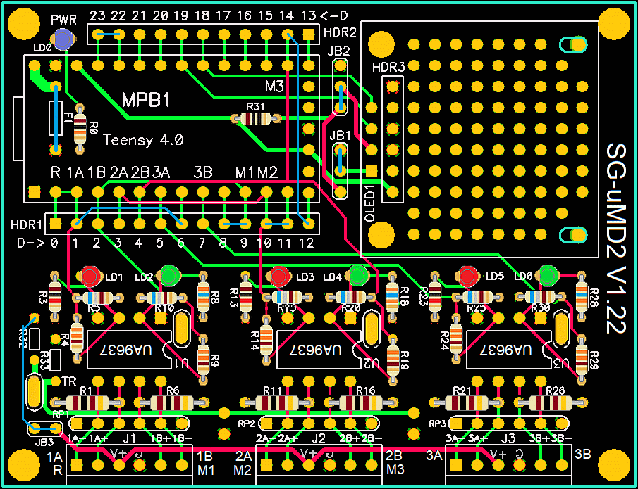
SG-µMD2 V1.22 PCB Layout Diagrams with 100 & 150 Ohm Terminators (Left), Minimal Single Axis V1.00 PCB, and Three Axis Populated V1.00 PCB with OLED Display (Right) (JB1 and JB2 Jumpered on Layout Diagrams for OLED GND on the Left and VCC on the Right)
(All kits going forward will have red and green LEDs for the A and B signals;
the original prototype was all boring green. Please pay attention to the
values for the current limiting resistors as they differ by more than an order
of magnitude for the red and green LEDs to equalize their perceived brightness.
Where the signal LEDs are all green, the R3,R8,R13,R18,R23,R28 will be 10K
ohms.)
In addition to the resistor color codes and component references, the
layout diagram also shows the signal locations for homodyne
and heterodyne on the Teensy.
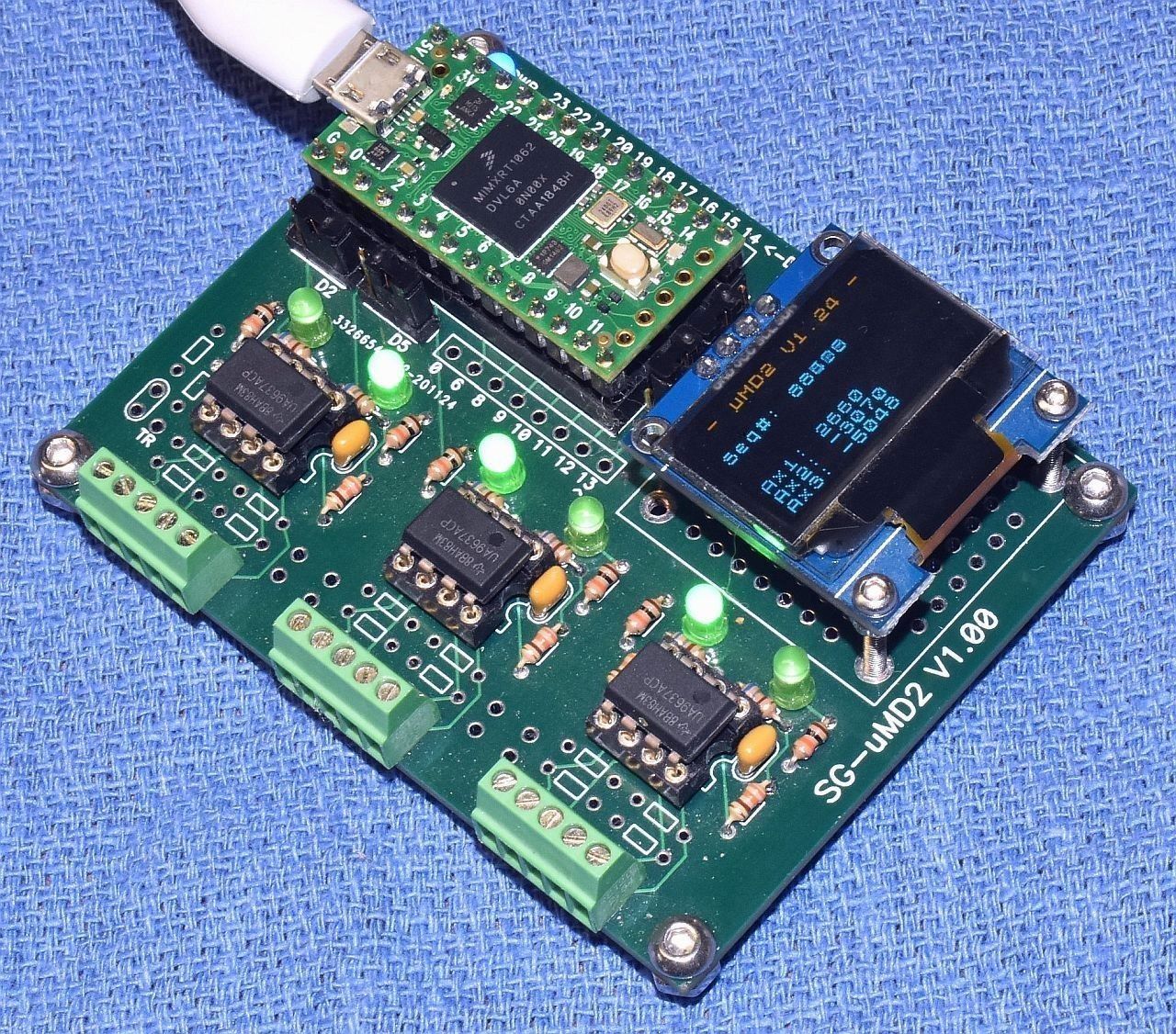
The populated PCB shows all components required for a three axis system
with the OLED display. The terminating resistors (near the screw terminal
blocks) have not been installed since their value may depend on the specific
configuration, and can often be left out. Five pin headers may be substituted
for the screw terminal blocks if desired. The signal LEDs shown are all
green in the photo, sorry. :) (These show the V1.00 PCB, updated versions
will be forthcoming.)
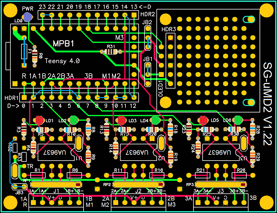
The following show the locations of all of the possible wire jumpers that
may be needed.
SG-µMD2 V1.22 PCB Layout Diagrams with Jumpers (Blue); 100 Ohm Terminators (Left) and 150 Ohm Terminators (Right)
Jumper Description (in blue)
F1 (upper left): This is required
and provides +5 VDC (Vcc) to the components on the
PCB as well as optional external power to encoders and the like. If not
using external power, it can be a wire.
JB1, JB2 (top center): OLED power select determines which pins
VCC and GND are on. Only required if the OLED is installed. Shown jumpered
for VCC on the right and GND on the left. Double check this for your
OLED! Getting it wrong will probably blow the OLED.
Heterodyne Interpolation (HDR1 and HDR2): Teensy pins D1 to D6,
D8 to D9, D10 to D11, D12 to D14. Only required if heterodyne interpolation
is enabled. The presense of these jumpers will not impact normal operation.
External power (lower left): Ooops jumper to connect +5 VDC to the
pins on the terminal blocks/connectors for encoder power. Only required
if encoder(s) will be powered from this board.
Homodyne/heterodyne firmware select (HDR2): Jumper between
Teensy digital pins 22 and 23 to select heterodyne firmware (installed).
Future option, not currently implemented.
Print out this document so each step can be checked off ( ) as it is completed.
The parts list below assumes populating the SG-µMD2 for 3 homodyne
axes with the OLED display. So for a single axis system, some parts
in this list may not be present and/or there is no need to install those
associated with channels 2 and 3 and/or for the OLED. Note that a 3-axis
heterodyne system requires the same peripheral parts as a 2-axis homodyne
system.
IMPORTANT: The color of the OLED display (if present) may be yellow/blue
(yellow for first two lines of text with blue for the remaining 6 lines),
all blue, or all white. In addition and more importantly, they may differ
slightly in their pinout and mounting hole type/location as follows (viewed
with the pins at the top):
Type 1: GND on the left and VCC (V3.3) on the right.
The mounting holes are round.
Type 2: VCC (V3.3) on the left and GND on the right.
The mounting holes are elongated.
There may be other variations. The kits will generally have the Type
1 yellow/blue OLEDs.
( ) Confirm that all parts are present and undamaged:
Core Parts:
( ) 1x blank SG-µMD2 V1.22 PCB. Confirm the version on the
silkscreen along the right edge of the PCB. Inspect for plating
or other defects.
( ) 1x Teensy 4.0 in antistatic bag. These are currently shipping
with V2.20 heterodyne firmware.
( ) 1x 28 pin wide DIP socket or 40 pin SIPP socket strip to trim to
a pair of 14 pin SIPP sockets.
( ) 2x 14 pin SIP male-male socket strip for Teensy, may need
trimming. Only included if Teensy doesn't already have pins soldered.
( ) 1x 3 mm blue LED.
( ) 1x 10 ohm 1/8 W resistor (brown-black-black-gold).
( ) 1x 10K ohm 1/8 W resistor (brown-black-orange-gold).
( ) 1x USB A to USB Micro B cable.
Peripheral Parts (1-Axis):
( ) 1x 6 pin screw terminal block or 6 pin header with shell and pins.
( ) 1x UA9637 or UA9639 line receiver (8 pin DIP in foam or tube).
( ) 1x 8 pin DIP socket.
( ) 1x 0.1 µF ceramic capacitor (marked with 104 or 0.1).
( ) 1x 3 mm red LED.
( ) 1x 3 mm green LED.
( ) 2x 100 ohm 1/4 W or 1/2 W resistor (brown-black-brown-gold).
( ) 1x 6 pin SIPP 150 ohm resistor pack (five 150 ohm resistors with
common connection) XOR 4 150 ohm 1/8 W resistors (brown-green-brown).
( ) 2x 330 ohm 1/8 W resistor (orange-orange-brown-gold).
( ) 2x 680 ohm 1/8 W resistor (blue-gray-brown-gold).
( ) 1x 1K ohm 1/8 W resistor (brown-black-red-gold). (1)
( ) 1x 0.96" 128x64 OLED IIC display in antistatic wrap or bag. It
will have its pins soldered.
( ) 1x 4 pin SIPP male-female socket strip.
( ) 2x M2x16 screw.
( ) 6x M2 nut.
For a two or three axis homodyne system, the Peripheral Parts quantities
will be multiplied by 2 or 3, respectively; for a three-axis heterodyne
system, the Peripheral Parts quantities will be multiplied by 2. And the
OLED parts will not be present, uh, for a system without the OLED. :)
The "Optional" parts identified below
can be omitted if that feature is not being
implemented. The LEDs especially are not really
that useful and with the default current limiting resistors, annoying bright.
So you may want to at least experiment with higher values of resistors
to tame them.
IMPORTANT: LEDs are really fragile with respect to soldering and tend to
die open easily. Make sure the leads are not stressed when heat is
applied - the LED should be able to jiggle slightly in the holes - and
keep the iron on them for as little time as possible.
( ) Install F1 (1 amp fuse) or jumper. This will normally just be a
jumper. But where the PCB is feeding +5 VDC power to an external encoder
or the like, a fuse should be used (normally not included in the kits).
( ) Install R0 (10K ohms) under where the Teensy socket will go.
( ) Install R31 (10 ohms) under where the Teensy socket will go.
( ) If there is a large DIP socket, it is for
for MPB1, the Teensy 4.0, and may need to be trimmed to 28 positions.
Rather than the DIP socket, there may a 40 pin deep socket strip requiring
cutting and trimming, or a pair of 14 pin deep socket strips that my just
require smoothing at the ends.. If cutting is required, DO NOT attempt
to slice it between pin positions - sacrifice one position and then file
the ends smooth.
( ) Carefully insert the socket or strips
into the PCB confirming no bent pins. For the socket, rather
than flipping a coin :), orient it so the large cutout faces the USB to
the left. Then solder
two corners and confirm it seats flat, then solder the other pins. Inspect
for solder bridges and unsoldered pins. For the stips, take care that
they are straight up and flush with the PCB before soldering. Then solder
the end pins, check that it seats properly, then solder ALL the other pins.
DO NOT attempt to plug in the Teensy until ALL pins are soldered.
( ) Install the 8 pin sockets for U1 (single axis) and U2,U3 (three axes).
Note orientation - the cutout goes to the right as viewed in the layout
diagram. Solder and inspect for solder bridges and unsoldered pins.
( ) Install C1 (0.1 µF, single axis) and C2,C3 (three axes).
C1,C2,C3 are the oval outlines to the right of U1,U2,U3 respectively.
( ) Install R4,R9 (330 ohms, single axis) and R14,R19,R24,R29 (three axes).
( ) Install R5,R10 (680 ohms, single axis) and R15,R20,R25,R30
(three axes).
( ) Install LD0 (3 mm blue LED). The anode is the longer lead
and goes to the right as viewed in the layout diagram. The flat is the
cathode and goes to the left. Cut the leads about 1/10" from the body
if the LED can't be inserted to sit flush on the PCB. Take care not
to overheat or stress the leads on the LED when soldering. Be as quick
as possible.
( ) Optional signal LEDs:
( ) Install R3 (single axis) and R13,R23 (three axes).
( ) Install R8 (single axis) and R18,R28 (three axes).
The actual value of R3, R13, and R23 for the red LEDs may range from
1K ohms (brown,black,red) to 2.2K ohms (red,red,red) depending on available
stock.
The most common value will be 1K ohms.
The actual value of R8, R18, and R28 for the green LEDs will depend
on whether the LEDs are normal or high brightness. For normal brightness
LEDs, the resistor values may range from 1K ohms (brown,black,red,gold)
to 2.2K ohms (red,red,red,gold), same as for
the red LEDs. For high brightness green LEDs, the resistor values may
range from 22K ohms (red,red,orange,gold) to 47K ohms
(yellow,violet,orange,gold).
The bottom line is that if there are no resistors greater than
2.2K ohms, the resistors for the LEDs will all be the same value between
1K and 2.2K ohms. ;-) No other resistors are in that range. If there
are resistors with a value of 22K ohms or higher, they will be for the
green LEDs.
If there appears to be ambiguity with respect to the green LEDs, it is
simple to test one using a 5 VDC power supply or 9 V battery: Connect
the resistor to + and then to the longer lead of the LED; connect the
shorter lead to -. A super bright green LED will be blindingly
bright on a 1K to 2.2K ohm resistor, way too bright to be an indicator! ;-)
( ) Install LD1 (3 mm red LED, single axis) and LD3,LD5 (three axes).
( ) Install LD2 (3 mm green LED, single axis) and LD4,LD6 (three axes).
The anode is the longer lead
and goes to the right as viewed in the layout diagram. The flat is the
cathode and goes to the left. Cut the leads about 1/10" from the body
if the LED can't be inserted to sit flush on the PCB. Take care not
to overheat or stress the leads on the LED when soldering. Be as quick
as possible.
( ) Install J1 (screw terminal block, single axis) and J2,J3 (three
axes). Make sure the entrance holes for the wires face away from the
PCB! Solder the center pin and confirm they are flat on the PCB, then
solder the others. Check for solder bridges and unsoldered pins.
6 pin headers may substituted for the screw terminal blocks if desired.
( ) Carefully inspect for unsoldered pins, solder bridges and
other blemishes. Correct as needed. THIS IS ESSENTIAL!
It would be bad form to blow the brain due to an errant blob of solder. :(
( ) Test the Teensy before doing anything to it. If it fails this test,
contact me before proceeding.
Connect it to a USB port using the USB A to USB Micro B cable.
Assuming the µMD2 firmware has been installed, after a
second or so, digital pin D13, the on-board LED, acts as a
heartbeat monitor and
should start flashing in some pattern not yet fully determined, but
it will be unlike the "Blink" sketch. ;-) Currently it's a short flash
ever 0.5 to 1 seconds.
IMPORTANT: Don't assume the Teensy has the correct firmware! Since the same
kit is used for both homodyne and heterodyne but the firmware differs.
Load the correct firmware before proceeding beyond this point. The
version can be confirmed in the µMD GUI, below.
It should also be spitting out data via the USB COM port. In the
Arduino IDE, go to Tools->Port and select the port that it is plugged
into. It should show something like: COM5 "Serial (Teensy)".
Go to Tools-Serial Monitor. A window should appear showing data
being sent to the COM port. It will be mostly boring but the 6th value
should be incrementing by 1, probably at around 1 kHz:
(Should you care, the 6th and 7th values are the "Low Speed Code" and
"Low Speed Data", respectively. 10,124 is the firmware version 1.24;
8,100000 is the sample rate of 1,000 x 100, and 20,4099 specifies 3 homodyne
axes + a homodyne multiplier of 4 x 256. Homodyne firmware has version
numbers of 1.xx. For heterodyne it is 2.xx, and combined homodyne and
heterodyne when available will be 4.xx.
Unplug the USB cable.
( ) Assemble the Teensy 4.0 PCB to the pin or socket strips. There will
either be a pair of 14 pin female-male socket strips precut or the male to
male pin strip that needs cutting. These steps are needed ONLY if the
Teensy does not already have pins soldered.
Female to male socket strips: The male pins slip through the
Teensy PCB holes from the top so the female sockets are accessible when
Teensy is plugged into the large socket on the SG-µMD2 PCB.
Male to male pin strip: The short pins slip through the Teensy PCB
from the bottom. (This is what's shown in the photo of the completed
SG-µMD2 PCB, above.)
Solder a single pin near the center and
confirm it seats flush, then solder the rest.
To assist in alignment, the strips can be inserted in the 28 pin socket
taking care not to push any of the individual pins out of position.
( ) Test the Teensy as above before plugging it into the SG-µMD2 PCB
to confirm the soldering hasn't done anything bad. Then unplug the USB
cable.
( ) Carefully plug the Teensy into the 28 pin socket. The USB socket
faces off the left side of the PCB as shown in the layout diagram.
Make sure all pins are seated and none are hanging off the socket.
CAUTION: Make sure all the pins line up with their entry points in the
socket to avoid squashing the leaf sprint contacts.
( ) Reattach the USB cable. The power LED should come on immediately
and after a second or so, the Teensy LED should start flashing as before.
Unplug the USB cable.
( ) Plug a UA9637 or UA9639 IC into the U1 position. The dot or cutout
should face to the right - these ICs are upside-down compared to the
Teensy part labeling as shown in the layout diagram. Confirm that no
pins are bent over.
( ) Reattach the USB cable. The power LED and possibly one or both
LEDs near U1 (if installed) should come on immediately
and after a few seconds, the Teensy LED should start flashing as before.
( ) (Optional) Here is the nifty bit. ;-) Moisten a finger (doesn't matter
which one) and touch the pins on J1. With some practice, it will be possible
to make the LEDs near U1 to go on and off as the input to the line receivers
cause them to toggle. While the behavior is not really predictable, just
the fact that they change indicates the the line receiver is working.
Since the UA9637 has some hysteresis, it latches but the slight charge
from your electric personality is enough to toggle it. CAUTION: Don't
get carried away, these parts can be damaged by static discharges.
So, no cat's fur and plastic rods, please. :( ;-)
(This will not be possible if the terminating resistors are installed, thus
holding off on them for now.)
If you're wondering how the OLED in the photo, above, can be displaying
such large numbers with nothing attached to the inputs, it was done this
way except the board was plugged in a USB charger, not a USB port. That must
have a lot of ripple relative to my moistened finger, enough to easily
trigger the UA9637 even with its hysteresis.
( ) Start the µMD GUI and select the COM port used to upload
the firmware. The graph should start scrolling. But now, if you do the
moistened finger thing, it should be possible to get the displacement
to change for Axis 1. Once confirmed, unplug the USB cable.
( ) Repeat the previous 3 steps for axes 2 and 3 (U2/J2 and U3/J3)
if installed.
( ) Heterodyne systems ONLY and ONLY if Interpolation is enabled in
the GUI. Add the following jumper wires on the
bottom of the SG-µMD2 PCB on the headers as required depending
on the number of axes. Use thin insulated wire and take care to avoid
solder bridges. The second attachment point for each jumper can be to
the appropriate labeled header pad. The following assumes the use of
V2.xx or later firmware as interpolation does not exist before then.
"xx" to be determined. Jumpers are shown in blue going to the
two long headers on the diagrams below.
Single axis:
( ) Install jumper for REF: D1 to D6. (MPB1 socket pins 3 to 8.)
( ) Install jumper for MEAS1: D8 to D9. (MPB1 socket pins 10 to 11.)
Three axis:
( ) Install jumper for MEAS2: D10 to D11. (MPB1 socket pins 12 to 13.)
( ) Install jumper for MEAS3: D12 to D14. (MPB1 socket pins 14 to 16.)
( ) Optional OLED:
( ) Install the 4 pin female-male socket strip (or a 4 pin piece of
a longer one trimmed appropriately) for the OLED between JB1 and JB2
and HDR3.
( ) Install wire jumpers to select V3.3 and GND for the
OLED at JB1 and JB2 depending on which version you have. The outer positions
select V3.3/VCC on the left while the inner positions select V3.3/VCC
on the right. These are also shown in blue for the case where VCC
is on the right. DO NOT plug in the OLED
until correct power connections are confirmed with a DMM:
               OLED Type 1         OLED Type 2
             GND VCC SCL SDK     VCC GND SCL SDK
                    o                   o
                                        |
                JB2 o               JB2 o
                    |
                    o                   o


                    o                   o
                    |
                JB1 o               JB1 o
                                        |
                    o                   o
CAUTION: DO NOT jumper the middle pins together by accident, that will
short V3.3 to GND. :( This should be impossible on the V1.22 PCB layout
but one can be really resourceful when not thinking things through
completely. :( :) Note: The jumper block numbering has changed between
PCB V1.00 and V1.22.
( ) If the OLED does not already have a 4 pin header attached,
cut off a 4 pin section of male-to-male pin strip and insert it under
the OLED with the short side through the OLED PCB just as with the
Teensy. Solder one pin, confirm it seats flush,
and solder the rest. Inspect for solder bridges and unsoldered pins.
( ) Insert an M2x16 mm screw through each of the bottom holes of the OLED
and thread an M2 nut onto each, tighten the nut. Add an M2 nut to each
of the screws.
( ) Plug the OLED into the 4 pin socket strip.
( ) With the screws protruding through the slots in the PCB. Adjust the
position of the loose nuts so the OLED is horizontal, then add 2 more M2
nuts and tighten them.
( ) Power up the PCB via the USB cable. After a second or so, the OLED
should display something like "µMD2 V1.xx" on the top line and
the sequence number on the 3rd line incrementing at the sample rate
(probably 1 kHz). These OLEDs can display 8 lines of text; for the version
provided in these kits, the top two are yellow while the other 6 are blue.
It is NOT a color display.
( ) Using the moistened finger trick :), it should be possible to fool the
system into thinking there is activity on each of the installed axes
at which point lines will appear on the OLED with the relevant axis ID
and count. This can be more fiddly than might be assumed as the Quadrature
counting hardware of the Teesny will ignore sequences of A and B that don't
make sense.
( ) (Optional) Termination. There are 3 options, see description, above
and below. Where the driver is DC-coupled (using an IC direct, normally used
with commercial homodyne systems), the 100 ohm termination
which is between the two outputs should be satisfactory. Where it is
AC-coupled (capacitor or transformer, normally with heterodyne systems),
the 150 ohm termination to GND should be used. If in doubt or for the
combined homodyne and heterodyne kits, install a
suitable socket. (Not included.) So, only one of the following
may be required:
( ) Heterodyne: Install RP1 (5x150 ohm SIP, single axis) and RP2.
(two or three axes). These are the 150 ohm termination resistor packs with 5
resistors tied to a common at pin 1. Due to an error on the V2.22 PCB
(can you believe it only took 3 or 4 years for someone to notice?!),
they must be installed with pin 1 on the right. There should be some
indication of pin 1 on the package. Pin 1 is denoted by a
dot which may be separate or at the left side of the lettering. Or test
with a multimeter. IMPORTANT: This is opposite of how the PCB is labeled,
oops.
Where there are four discrete 150 ohm resistors instead of the SIP terminator,
install them in the center 4 locations tied together and connected to
the hole at the right end of the SIPP pattern.
Alternate: Where there is a common ground between µMD2 and the
power supply for the optical receiver (as there will almsot always
be), R1,R6 (100 ohm, 1/4 watt, single axis) and R11,R16,R21,R26,
three axes) may be installed instead, just like for homodyne (below).
( ) Commercial homodyne or DIY homodyne with RS422 driver: Install
R1,R6 (100 ohm, 1/4 watt, single axis) and R11,R16,R21,R26, three axes).
( ) Any system with single-ended output and short cable: No
termination is required but it will be necessary to set up the
"Reference Voltage". See the next section.
If in doubt, cut the female-male socket strip
into pieces and solder them in so alternative termination schemes
can be tried without requiring unsoldering.
( ) (Optional) External power. Pin 3 of J1,J2,J3 is for +5 VDC power
to external hardware line encoders. Since it comes from USB, the current is
limited to the capacity of the USB port minus what is used by the hardware
on the PCB. Pin 3 on J1,J2,J3 is connected to JB3-2 located at the lower
left of the PCB. JB3-1 was supposed to be +5 VDC on the PCB but apparently
the last revision of the netlist never made it onto the PCB, so pin 1
of JB3 doesn't go anyhwere. Oops. :( :) Add a jumper from JB3-2 to
the upper pin of R32. (If anyone reading this is old enough to remember
the imfamous 100 MHz Pentium floating point bug where FDIV returned
slightly incorrect results, this was a similar error of a block of
code not getting uploaded.)
Note: If normal (not high brightness) LEDs are installed in unused axis
locations, there may be slight "ghost" glow from them even when they should be
off due to leakage from +5V through to the the +3.3V of the Teensy pin. If
you're a purist and that bothers you (or just don't want to be distracted),
add a 1K ohm resistor between +5V (pin 1 of the UA9637/9) and the LED
cathode (pins 2 and/or 3).
Congratulations, you're all set to go. Order that construction crane
in need of a controller with free shipping on eBay. ;-)
Where the input signals are differential with approximately equal average
levels and an amplitude more than about 0.5 V, the UA9637 RS422 receivers
are all that's needed. This includes Quad-Sin-Cos which will automagically
convert to digital, but only if they have sufficient drive current.
Direct photodiode signals probably will not work without buffering.
But where the input signals are single-ended such as normal TTL or only
one polarity of a Quad-Sin-Cos, there are locations on the SG-µMD2
PCB for a reference voltage divider.
The threhsold voltage should be selected to be approximately mid-way between
the nominal high and low levels. For standard TTL, this would be 1.4 V. The
resistor values can be in the 10K range with C4 of 0.5 µF.
However, note that the line receivers have a relatively high input bias
current so they cannot be driven directly from a low current source like
a photodiode - an preamp must be used. Check the spec sheet if in doubt.
IMPORTANT: Due to a screwup on the PCB artwork, the +5 pad of R32 is NOT
connected. So a jumper to any nearby +5 pad will be needed. If you are old
enough to recall the Intel Pentium 100 floating point bug where a chunk of
microode never got downloaded, this is similar. The last bit of the netlist
was somehow omitted. :( :)
The Digikey
CART for SG-OR3 V1.02 PCB has most of the required parts
other than the Teensy 4.0 (available from Sparkfun) and SG-uMD2 PCB.
This can be edited to add or delete parts as desired. Where the quantity
is larger than required, it means the cost was probably lower. ;-)
And it's probably silly to pay exorbitant prices for common parts
like LEDs. Note: Due to an apparent bug in the Digikey Cart loader,
a few invalid part number errors may appear, but the parts will load OK.
Disclaimer: There may be errors in the CART! ;-)
Note: There are gaps in some part number sequences by design. ;-)
These are the required parts for up to a 3 axis system.
Some parts like the LEDs (along with their
associated current limiting resistors) can also be omitted if desired.
Refer to the schematic for more details.
 Reference   Type      Part/Value     Function
-------------------------------------------------------------------------------
    C1     Capacitor 0.1 µF           U1 5V bypass (3)
    C2*    Capacitor 0.1 µF           U2 5V bypass (3)
    C3*    Capacitor 0.1 µF           U3 5V bypass (3)
    C4     Capacitor 0.1 µF           Reference (TR) 5V bypass (3)

    F1     Fuse, 1 A                  AUX +5V fuse (optional)

    J1     Terminal Blk or Hdr 6 pin  1A/1B/REF/MEAS1 input
    J2*    Terminal Blk or Hdr 6 pin  2A/2B/MEAS2 input
    J3*    Terminal Blk or hdr 6 pin  3A/3B/MEAS3 input

   LD0     LED       3 mm LED        Blue Power LED

   LD1+    LED       3 mm LED        Red 1A/REF LED
   LD2+    LED       3 mm LED        Green 1B/MEAS1 LED
   LD3*+   LED       3 mm LED        Red 2A/MEAS2 LED
   LD4*+   LED       3 mm LED        Green 2B/MEAS3 LED
   LD5*+   LED       3 mm LED        Red 3A LED
   LD6*+   LED       3 mm LED        Green 3B LED

   MPB1    CPU       Teensy 4.0      Teensy 4.0 soldered to header

   PCB1    PCB       SG-µMD2-PCB     Blank SG-µMD2 V1.22 PCB

    R0     Resistor  10K ohm, 1/8 W   Power LED current limiting

    R1     Resistor  100 ohm, 1/4 W   IN1 termination
    R3+    Resistor  1K ohm, 1/8 W    1A/REF red LED current limiting (1)
    R4     Resistor  330 ohm, 1/8 W   1A/REF 5V->3.3 V level shift
    R5     Resistor  680 ohm, 1/8 W   1A/REF 5V->3.3 V level shift

    R6     Resistor  100 ohm, 1/4 W   IN2 termination
    R8+    Resistor  1K ohm, 1/8 W    1B/MEAS1 green LED current limiting (2)
    R9     Resistor  330 ohm, 1/8 W   1B/MEAS1 5V->3.3 V level shift
    R10    Resistor  680 ohm, 1/8 W   1B/MEAS1 5V->3.3 V level shift

    R11*   Resistor  100 ohm, 1/4 W   IN3 termination
    R13*+  Resistor  1K ohm, 1/8 W    2A/MEAS2 red LED current limiting (1)
    R14*   Resistor  330 ohm, 1/8 W   2A/MEAS2 5V->3.3 V level shift
    R15*   Resistor  680 ohm, 1/8 W   2A/MEAS2 5V->3.3 V level shift

    R16*   Resistor  100 ohm, 1/4 W   IN4 termination
    R18*+  Resistor  1K ohm,  1/8 W   2B/MEAS3 green LED current limiting (2)
    R19*   Resistor  330 ohm, 1/8 W   2B/MEAS3 5V->3.3 V level shift
    R20*   Resistor  680 ohm, 1/8 W   2B/MEAS3 5V->3.3 V level shift

    R21*   Resistor  100 ohm, 1/4 W   IN5 termination
    R23*+  Resistor  1K ohm, 1/8 W    3A red LED current limiting (1)
    R24*   Resistor  330 ohm, 1/8 W   3A 5V->3.3 V level shift
    R25*   Resistor  680 ohm, 1/8 W   3A 5V->3.3 V level shift

    R26*   Resistor  100 ohm, 1/4 W   IN6 termination
    R28*+  Resistor  1K ohm, 1/8 W    3B green LED current limiting (2)
    R29*   Resistor  330 ohm, 1/8 W   3B 5V->3.3 V level shift
    R30*   Resistor  680 ohm, 1/8 W   3B 5V->3.3 V level shift

    R31    Resistor  10 ohm, 1/8 W    V3.3 protect

    RP1    Resistor pack, 5x 150 ohm  IN1/IN2 Termination
    RP2    Resistor pack, 5x 150 ohm  IN3/IN4 Termination
    RP3    Resistor pack, 5x 150 ohm  IN5/IN6 Termination

   SKT1    Socket    14 pin SIP       Socket for Teensy 4.0
   SKT2    Socket    14 pin SIP       Socket for Teensy 4.0

   SKT2    Socket    8 pin, 300 mil   Socket for IN1/2/REF/MEAS1 line receiver
   SKT3*   Socket    8 pin, 300 mil   Socket for IN3/4/MEAS2/3 line receiver
   SKT4*   Socket    8 pin, 300 mil   Socket for IN5/6 line receiver

   SKT5+   Socket    40 pin, SIP      Socket strip for terminating resistors

    U1     IC        UA9637 or UA9639 REF/MEAS1 line receiver
    U2*    IC        UA9637 or UA9639 MEAS2/MEAS3 line receiver
    U3*    IC        UA9637 or UA9639 MEAS2/MEAS3 line receiver
"*" denotes parts that can be omitted for a single axis system.
"+" denotes parts that are not required for µMD2.
Notes:
The actual value of these resistors may be 1K to 2.2K ohms.
The actual value of these resistors may be 1K to 2.2K ohms XOR
22K to 47K ohms depending on whether normal or high brightness green
LEDs are included in the kit.
The 0.1 µF bypass caps do not have reference designators but
they are next to pin 1 of U1, U2, and U3.